
The schematic is where you define all the electrical connections. Think of it as the wiring diagram before you worry about physical placement.
#Open the schematic editor
- From the KiCAD project window, click the Schematic Editor button
(the icon that looks like a circuit diagram), or double-click your
.kicad_schfile.
#Adding symbols
#Bring in the core parts
-
Press A (or go to Place → Add Symbol) to open the symbol chooser.
-
In the search bar, type the part you want:
RaspberryPi_Picofor the Pico microcontrollerSW_Pushfor a key switchMX_stabfor a stabilizer (from marbastlib)1N4148for a diode
-
Select the symbol and click OK. It will attach to your cursor. Click to place it on the schematic.
-
Press Escape when you're done placing.

#Understanding the keyboard matrix
A full 60% keyboard has around 61 keys, but the Pico only has 29 GPIO pins, which is not enough for one wire per switch. The solution is a keyboard matrix.
In a matrix, switches are arranged in rows and columns. You only need one pin per row and one pin per column. A 6-row × 11-column matrix can handle 66 keys using just 17 pins.
To make the matrix work correctly, each switch needs a diode wired in series with it. Without diodes, pressing multiple keys at once causes "ghosting", phantom keypresses that shouldn't be there.
For a deeper explanation of how matrices work, see this guide.
#Wiring a switch-diode unit
#Wire one key
-
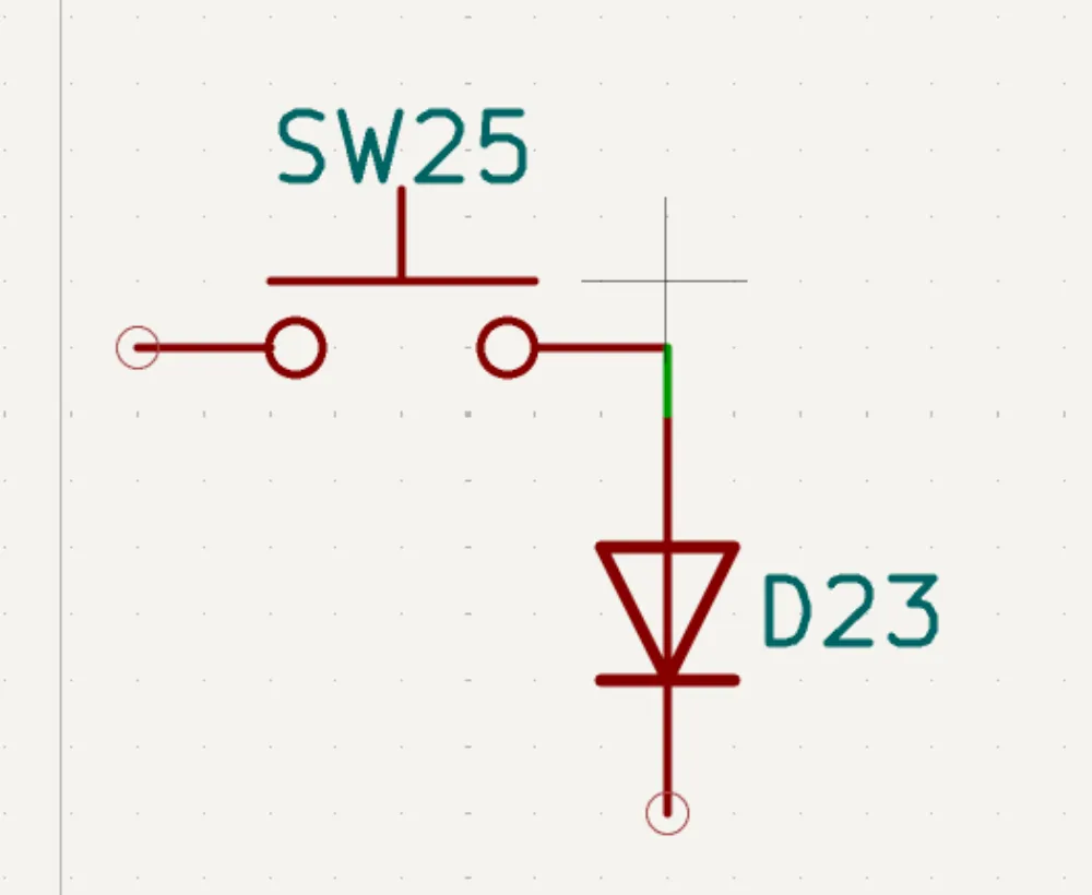
Each key is a pair: one switch and one diode. Wire them like this:
-
Place a
SW_Pushsymbol and a1N4148diode next to each other. -
Connect one leg of the diode to one pin of the switch using the Wire tool (press W).
-
The other leg of the diode connects to the row line. The other switch pin connects to the column line.
#Replicate for every key
-
Replicate the switch-diode unit for every key in your layout. Arrange them to match the physical layout of your keyboard from your sketch, with rows going left to right and columns going top to bottom.


#Using net labels
Instead of drawing a wire all the way from each row/column to the Pico (which would make the schematic unreadable), use Net Labels:
#Label rows and columns
- Press L (or go to Place → Net Label) to add a label.
- Name your rows
ROW0,ROW1,ROW2, etc. and your columnsCOL0,COL1, etc. - Attach matching labels to the corresponding pins on the Pico.
KiCAD treats any two wires with the same label as electrically connected, even if they aren't physically drawn touching. The small green dots you see are junctions that confirm two wires are connected. If wires cross without a dot, they are not connected.

#Adding stabilizers
Stabilizers need to be placed in the schematic too so they get footprints on the PCB.
Only add a stabilizer for each key that is 2u or wider (spacebar, backspace, left shift, enter). For a standard 60% layout, that's usually 3-4 stabilizers.
#Place MX_stab symbols
-
Press A and search for
MX_stab. -
Place one for each wide key in your layout.

#Adding mounting holes
If you're building a tray-mount case, add mounting holes to your schematic so they appear on the PCB.
#Add 4-6 mounting holes
-
Press A and search for
MountingHole. -
Place 4-6 holes around the edges and corners of where your board will be.
-
There are several mount styles, and each one changes the typing feel of the finished keyboard:

#Annotate
Before you can move to the PCB layout, every component needs a unique
reference designator (like SW1, D1, U1). This is called
annotation.
#Auto-annotate
-
Go to Tools → Annotate Schematic.
-
Leave the default settings and click Annotate.
-
KiCAD will automatically number all your components.

