
#The button footprint mismatch
After importing the button from EasyEDA, the footprint looks fine at first glance:

EasyEDA uses a redundant 4-pin symbol, showing all four pins even though two pairs are internally shorted:

KiCad uses a cleaner 2-pin representation:

When imported, EasyEDA's pins 1 and 2 land on opposite footprint pads - but on the physical switch they're on the same side, internally shorted. Pads that should be separate end up sharing a net, and the button does nothing because one side is permanently shorted to itself.
| EasyEDA pins | Physical side | KiCad net |
|---|---|---|
| 1, 2 | Side A (shorted) | Net 1 |
| 3, 4 | Side B (shorted) | Net 2 |
The switch connects Side A to Side B when pressed - the footprint must reflect that. Confirm with the datasheet from the product page:


#Fix the button pad numbering
-
Double-click the footprint in the PCB editor and choose Edit Library Footprint.

-
Renumber the pads: both pads on one physical side become 1, both on the other side become 2.

-
Ctrl+S to save, then Tools → Update Footprint from Library and click Update.

-
Not working? Delete the buttons and update from schematic again.

#Fix the XIAO footprint
-
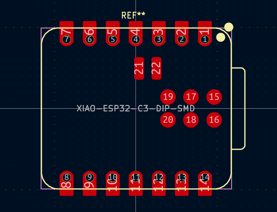
Same idea for the XIAO:
-
Double-click each BAT pad, set it to through-hole (THT), and give it a drill diameter of 0.889mm - that's what lets you solder the XIAO on by melting solder into the pads.

-
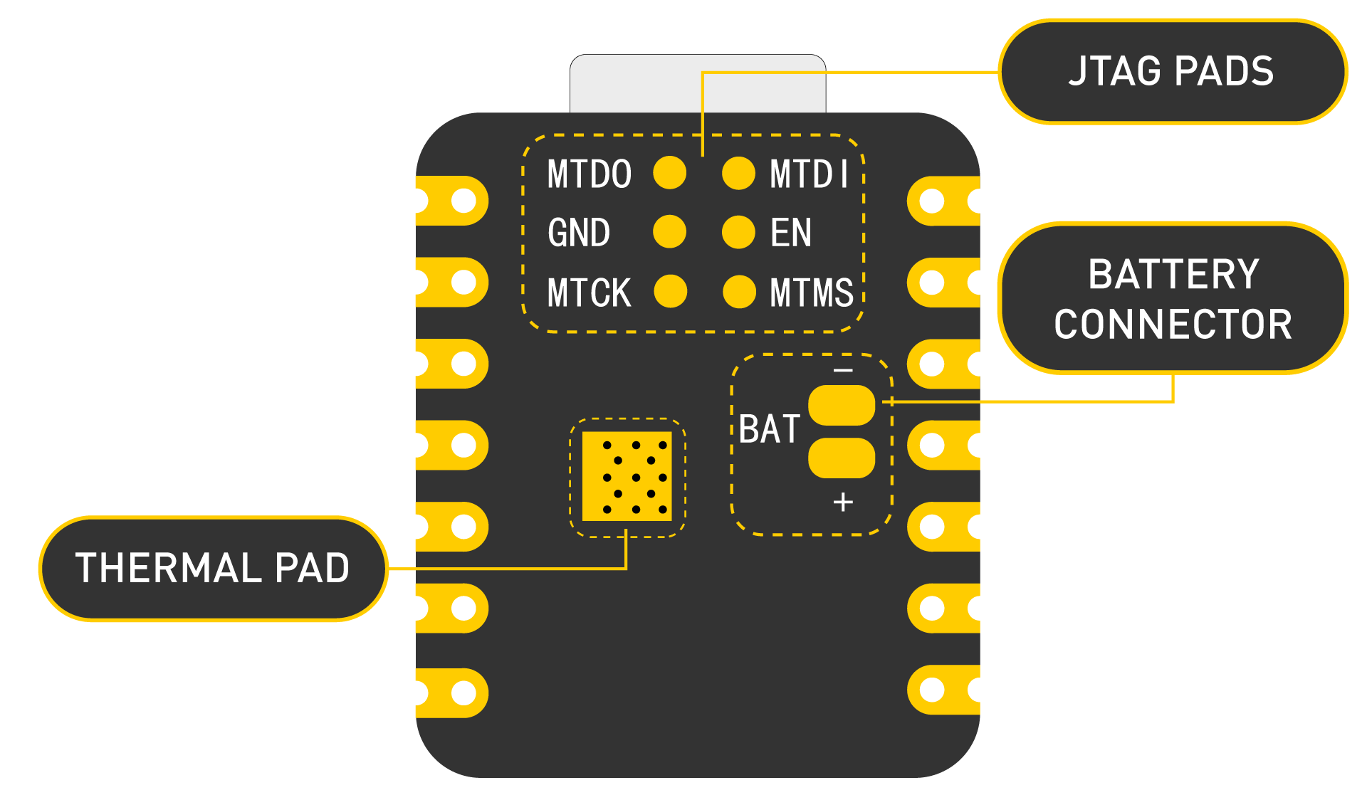
The pin numbers also disagree with the official Seeed diagram - fix them to match. The footprint is mirrored, so temporarily move it to the back layer to orient it the same way as the diagram:
-
Useful diagrams:

