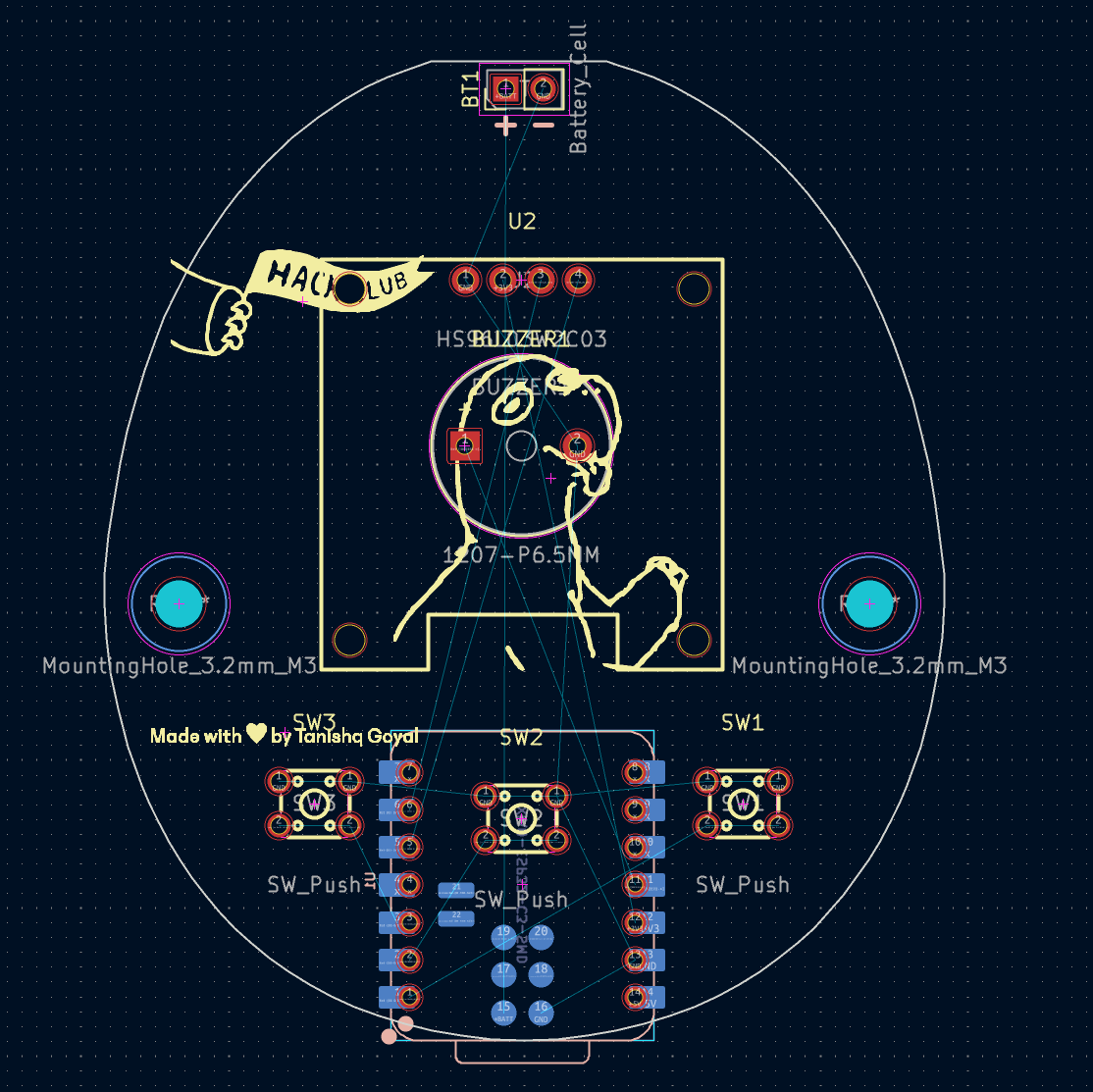
Opening the PCB editor, you should see something like this:

Any time you change the schematic, press F8 (or click Update PCB from Schematic) to pull the changes into the layout. The two circles you see are M3 mounting holes - press A to add your own.
#Define the board outline
-
The white outline is the Edge Cuts layer - the physical boundary where the PCB gets cut. Draw it by selecting
Edge.Cutson the right and using the drawing tools. -
Want something more custom than rectangles? This outline was drawn in Figma, converted with an image-to-DXF converter, imported into KiCad, then scaled against a 100 × 100 mm reference box using the measuring tool:

-
KiCad's own drawing tools work well too - a cool, unique border is worth the detour though. Try it!

#Place the components
-
Place every component inside the outline. The thin straight blue lines are ratlines (ratsnest lines) - unrouted connections showing which pads must eventually be joined by copper.
-
Arrange components so the ratlines are short and don't cross - that's the whole game, and it makes routing dramatically easier.
-
M moves, R rotates, F flips a component to the other side of the board, and Ctrl+S saves - do that often.
-
Here's the result: