
A PCB is made of layers. Our boards are "two-layer" - two sheets of copper with the substrate between them:
| Layer | Description |
|---|---|
| Top & bottom silkscreen | The white ink layer where you can add art |
| Top & bottom copper | The layers where you make your copper wires |
| Substrate | The actual plastic (usually green) which makes up your board |
| Via | The tunnels which connect the top and bottom copper layers |

#Route the traces
-
Hit X and click anything with a thin blue line poking out. The screen dims, shows the direction to go, and highlights the destination:

-
Join the highlighted points. If the front side is blocked, route on the back by selecting B.Cu in the right toolbar - or press V mid-route to drop a via, a tiny plated tunnel that carries the trace to the other side.
-
The rest of the routing vocabulary: Backspace deletes the last segment while routing, Esc cancels the route, D drags a trace without breaking connections, U selects a whole trace.
Your routing is complete!

A few notes on that screenshot: the red and blue fills are a ground plane - not required, but it helps routing, reduces noise, and looks nice. The small holes scattered across it are stitching vias - you do not need those, they're completely optional for a board like this.
#Customize the silkscreen
-
Click F.Silkscreen and use the text tool to add labels or jokes:

-
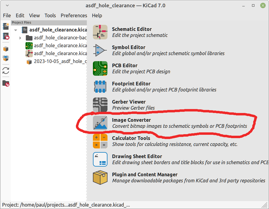
For art, select the top or bottom silkscreen layer and run your image through the KiCad image converter:
-
Your board is now beautiful.
#Run the Design Rules Check
-
DRC verifies the board has no interference errors, nothing off the board edge, and no intersecting wires. (It does not confirm the circuit works.)

-
Work through any errors it reports. The common families: clearance and track-width violations, via sizing, pad and hole clearances, board-edge and silkscreen issues, zone slivers, missing connections, and courtyard overlaps. Confusing ones? Ask for help - that's what the community is for.