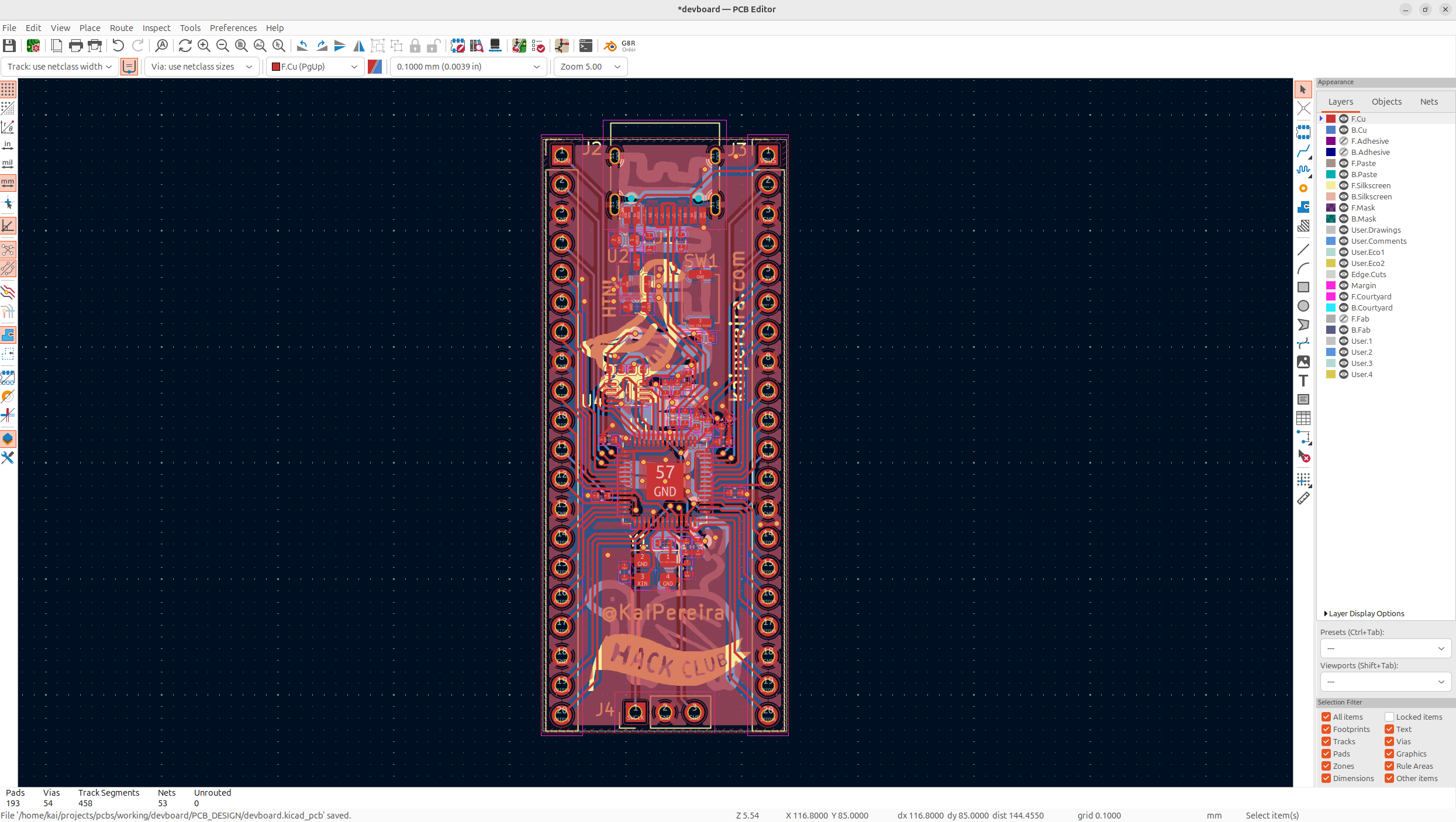
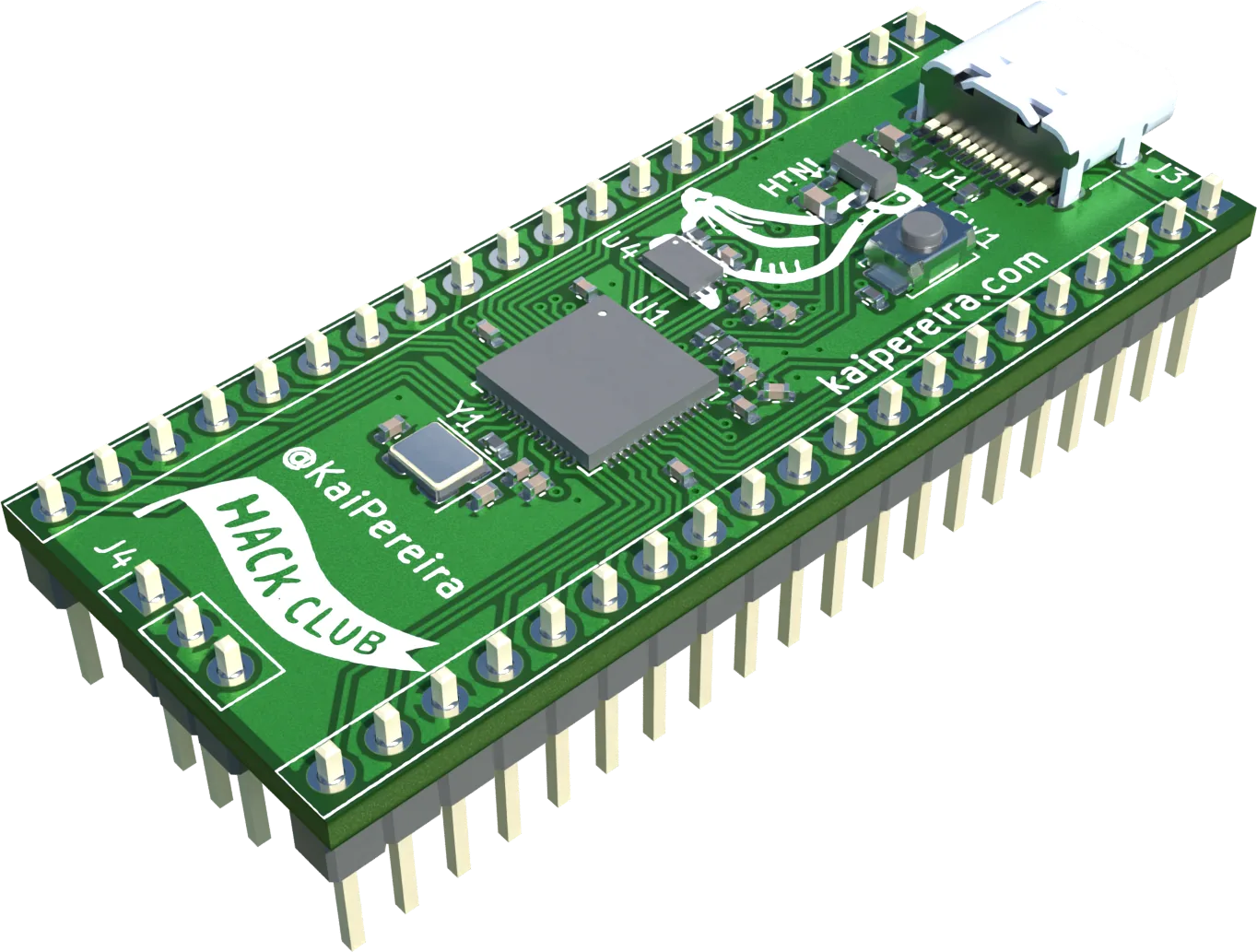

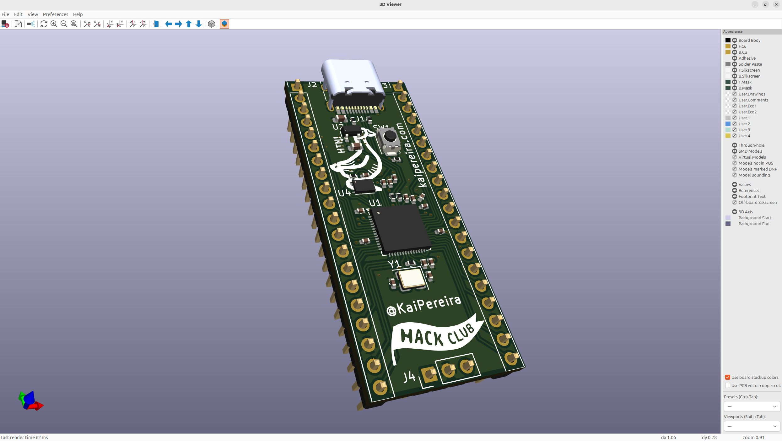
Today, we're going to be designing our own dev board, using one of the most popular and beginner friendly SoC's, the RP2040. This guide doesn't serve as just a tutorial, but also as an opportunity to learn what everything on the PCB fundamentally does, and what every single component on your PCB is actually for!
All the source files for this tutorial can be found here, so if you need any help, feel free to resort to the repository!
What you need
~$15 total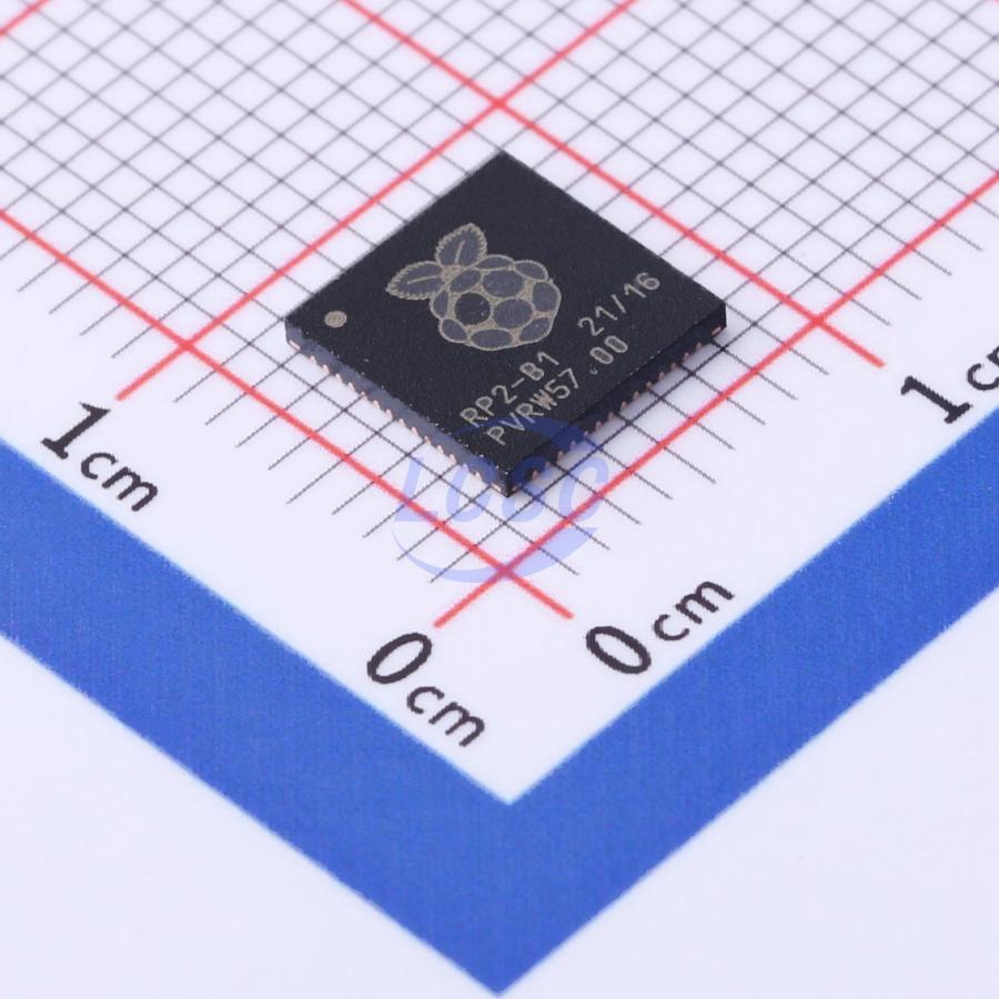 RP2040 SoCthe beginner-friendly SoC we're designing around1× · $1
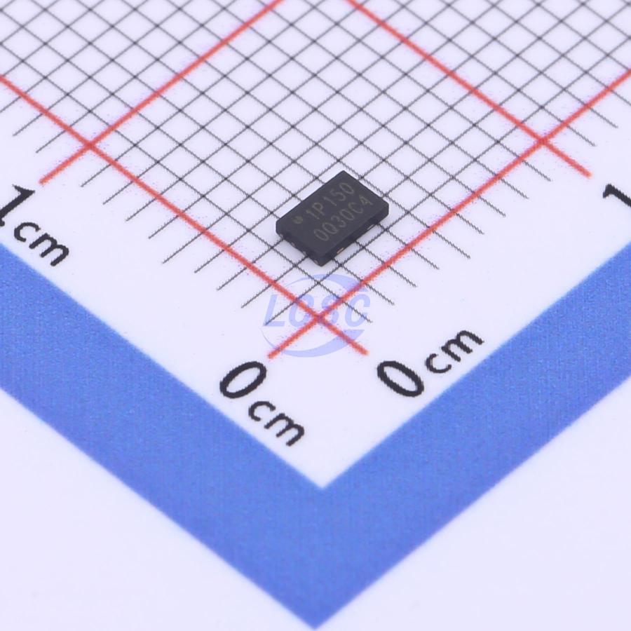 W25Q16JVZPIQ flash memoryquad SPI, same package the Pi Pico uses1× · $1
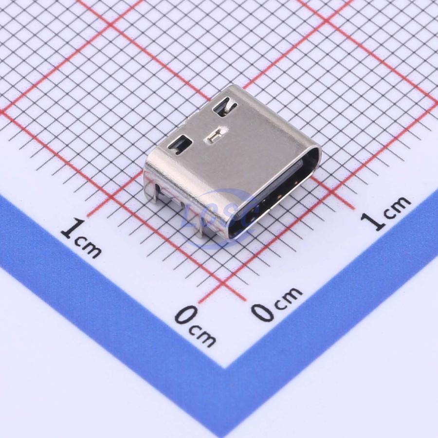 USB-C receptacleTYPE-C-31-M-12, JLC part C1659481× · $1
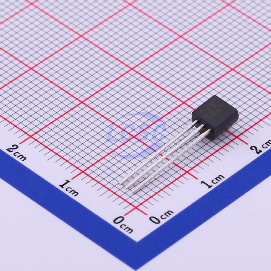 MCP1700-3.3 LDO3.3V fixed regulator, small SOT-23 package1× · $1
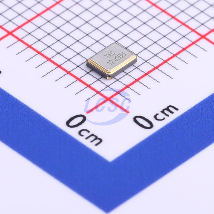 12 MHz SMD crystal4-pin 3225 package1× · $1
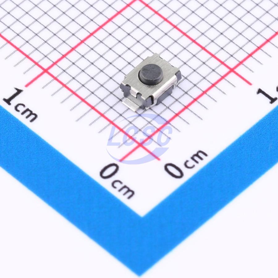 Tactile SMD buttonfor BOOTSEL1× · $1
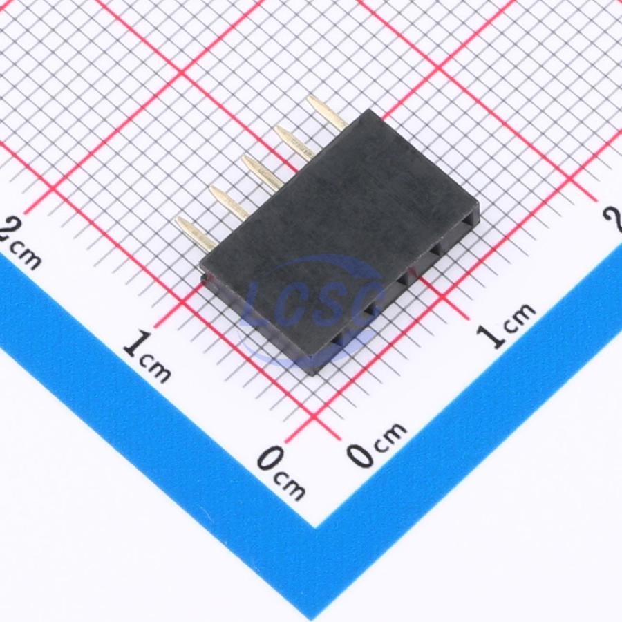 2.54mm pin headerstwo 1x20 and one 1x3 - matches the Pi Pico footprint1× · $1
 Passives (caps + resistors)0.1uF/1uF/10uF/33pF caps, 27Ω/1K/5.1K/10K resistors - JLCPCB basic parts1× · ~$1
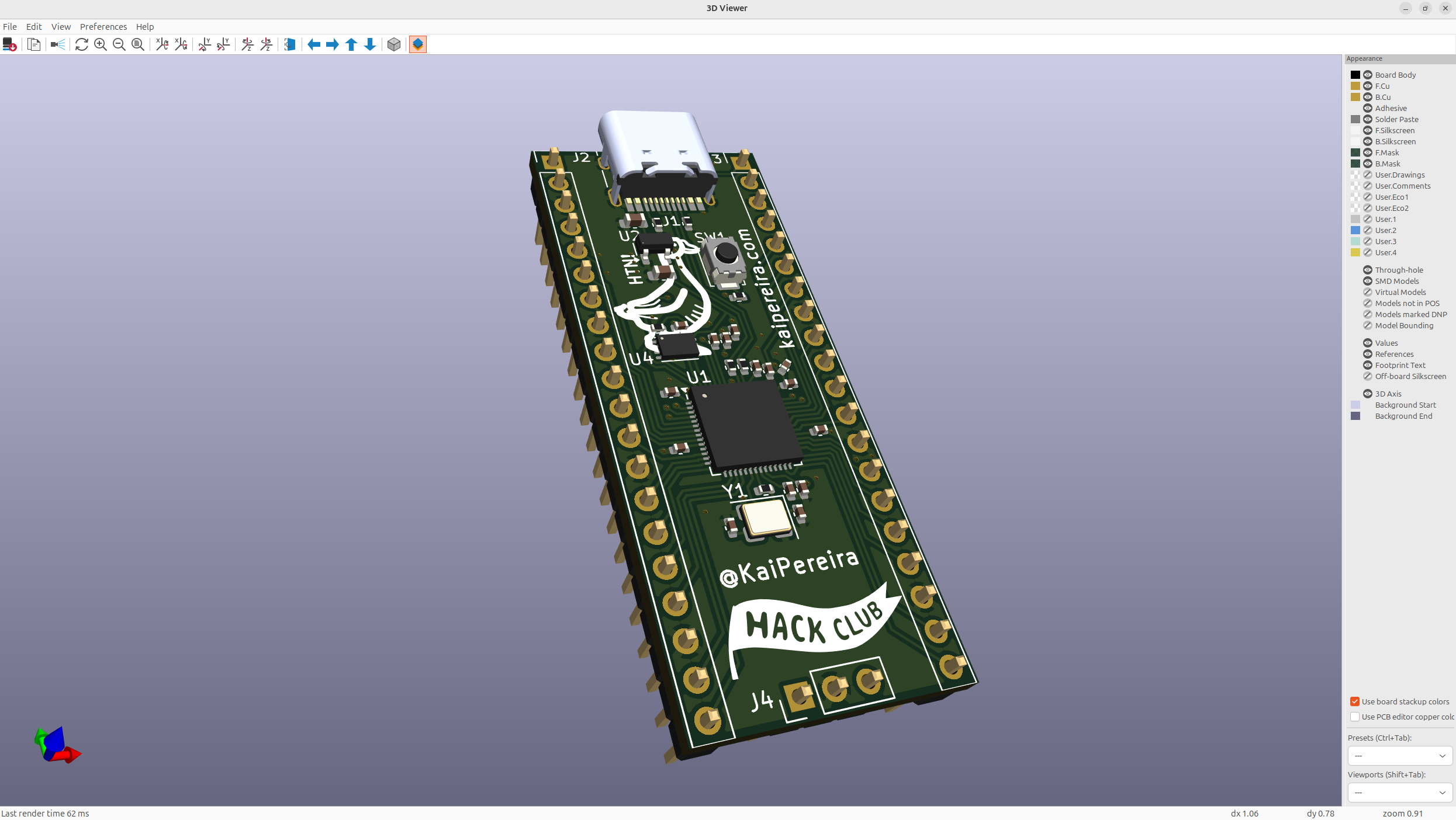 Your PCB, fabbed with PCBAJLCPCB, shipping included1× · ~$5
Now let's start off with the basic question, what's an SoC! An SoC or system on chip, basically has all the basic components like SRAM, processors, USB controllers, and other peripherals you'll break out onto your board. The RP2040 is a good SoC to start with, because the datasheets are simple, it's low-cost, has good on-chip memory and is really flexible with plenty of IO's.
Now let's get right into it, we'll be using KiCad for this tutorial, and I would suggest completing the hackpad tutorial and maybe a keyboard before trying to make your own devboard, not because you won't be able to make it, but you'll understand how it works a bit better.
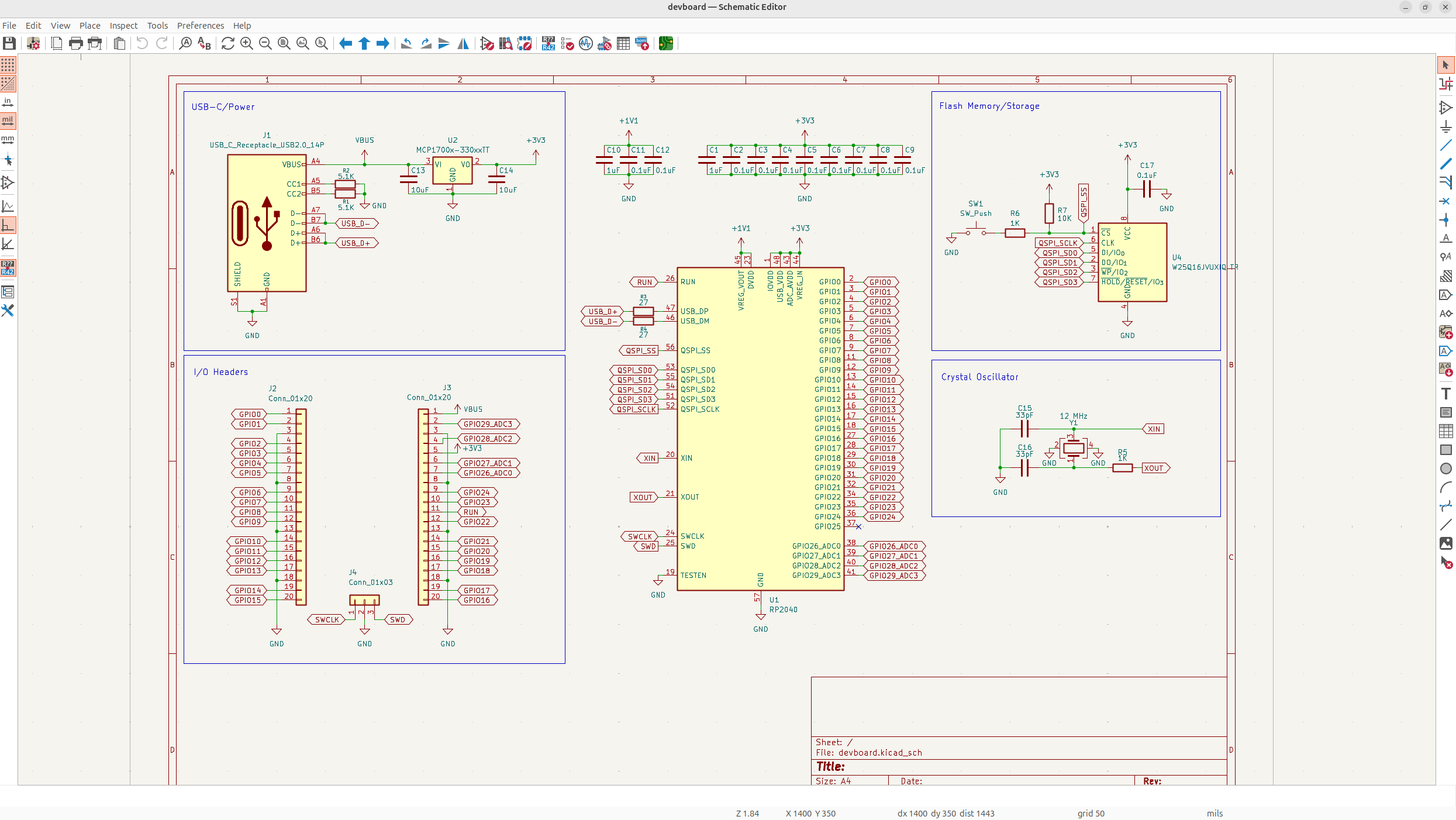
This is how our schematic will look when done the tutorial:
And this is the PCB editor: