So create a new KiCad project by going File → New Project, and choosing your name/folder for the project. After that, double click your schematic to start working on your PCB.
#Place the RP2040 symbol
-
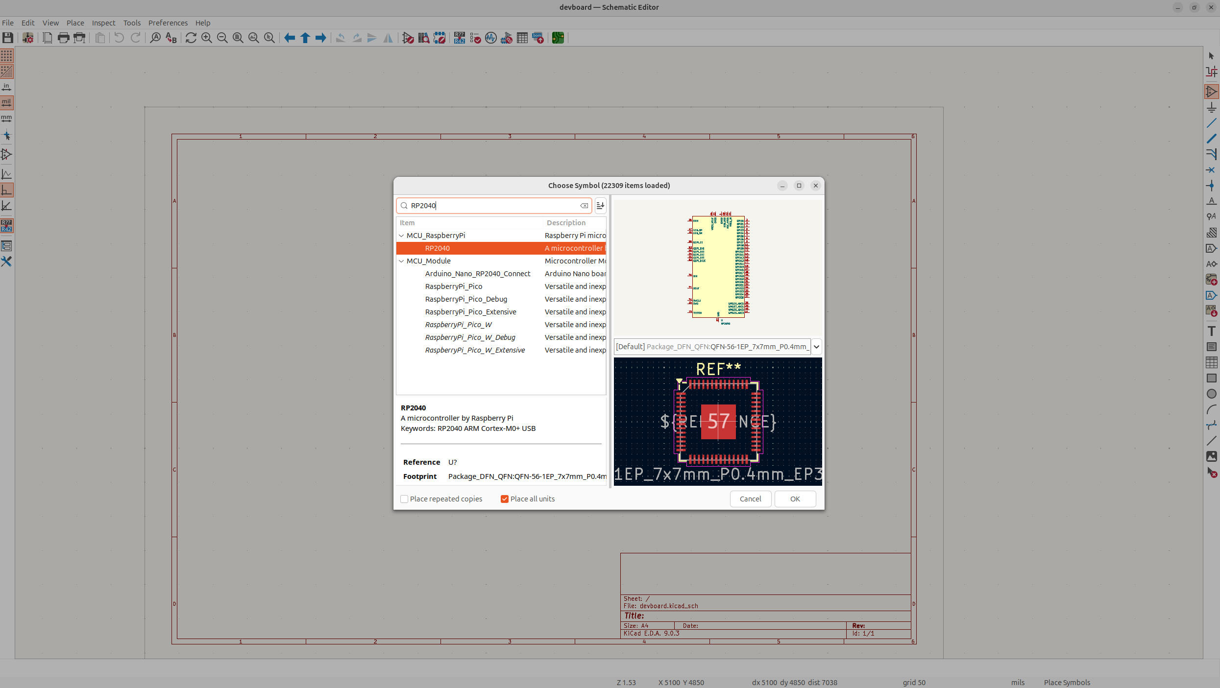
Enter your schematic, and then tap "a", this will open up the symbol library, which is the place where you can find component blocks that you'll wire together to form the schematic for your project.
-
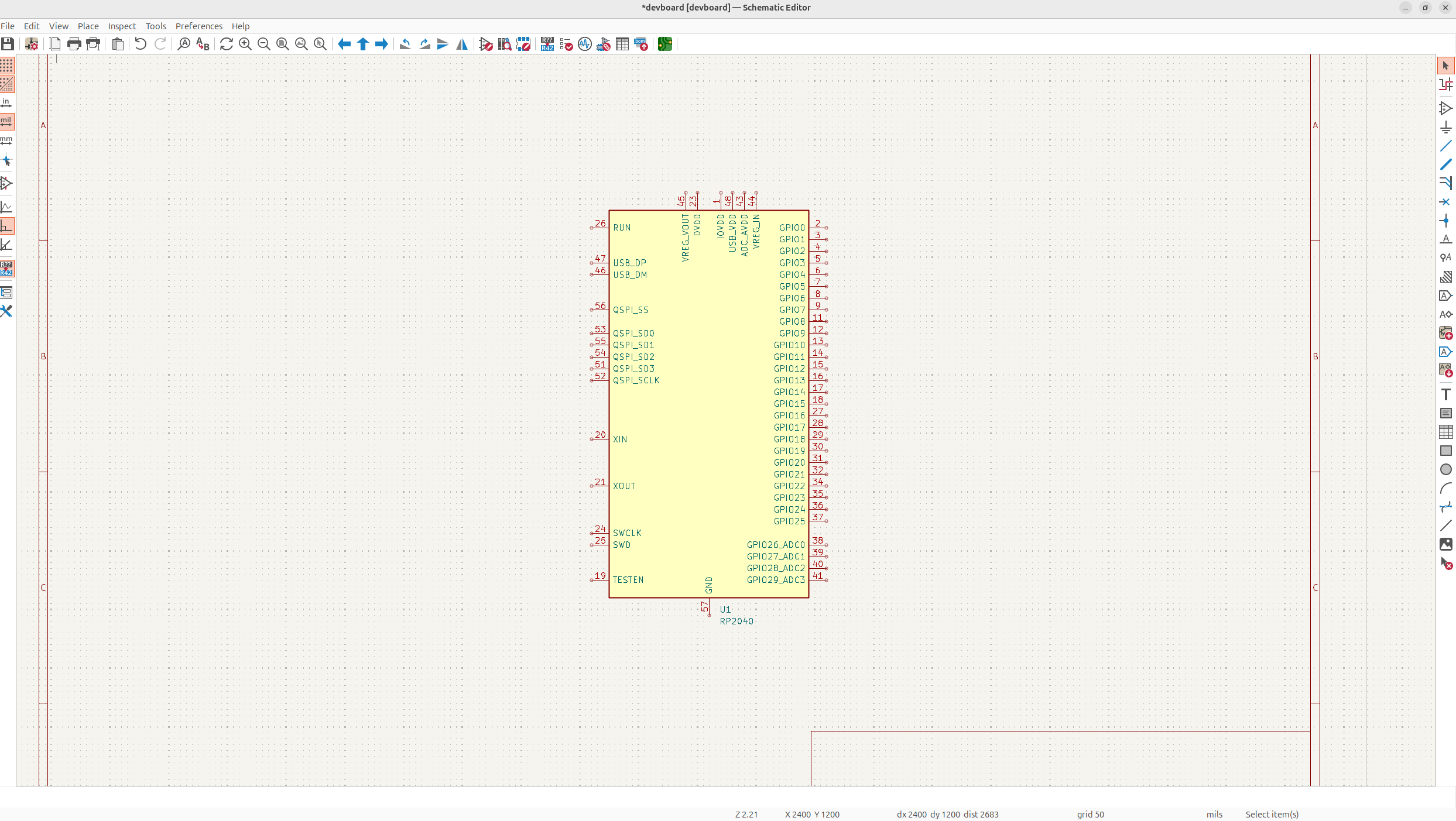
Search for the RP2040, and just place it down in the center of your schematic.
-
You'll notice the symbol and actual component are 2 different things if you look at the first screenshot. The symbol just tells you all the pins on the component, and how they'll be wired to what. The actual component has the physical pads where traces will actually connect to on your PCB!
Our entire schematic will consist of 5 main elements: power, flash storage, the crystal oscillator, I/O (input/outputs), and your SoC, the RP2040! The Raspberry Pi datasheet explains how all of this will pretty much be wired, and I'm kind of just here to explain exactly how it all works too.
#Power and decoupling
So first let's talk about power and some schematic good practices!
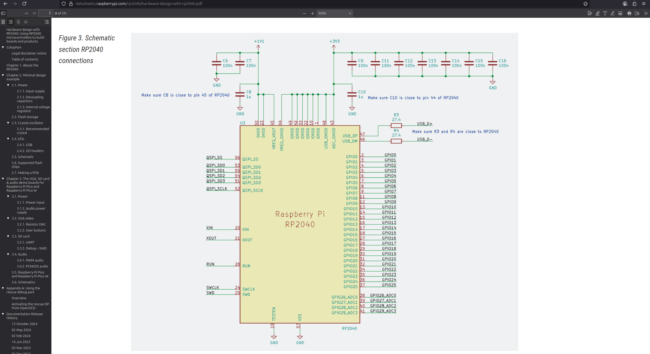
You'll notice that the RP2040 has capacitors, these are called decoupling capacitors. These capacitors are used for 2 main things, filtering out power supply noise and giving a local power supply if components need it at short notice. You can think of it like a stream of water, without the capacitors it can be jittery and unpredictable, but with the capacitors, the stream smooths out, making your PCB function more reliable.
You usually want to put one 0.1uF (or 100nF, the F stands for Farads) decoupling capacitor per power pin, but it's fine to deviate a bit from that, but that's the most optimal way of doing it and what we're going to do.
We're also going to put a 1uF decoupling capacitor on each power line. You'll notice that the RP2040 has a +1V1 (1.1V) and a +3V3 (3.3V) line, we want to put a 1uF decoupling capacitor per line, to act as a larger reservoir and to smoothen out larger ripples that could occur. With the RP2040, these 1uF capacitors are mostly to help provide a stable 1.1V supply. With this combination, we'll filter out nearly all the noise and have a smooth functioning PCB.
#Wire the power pins
-
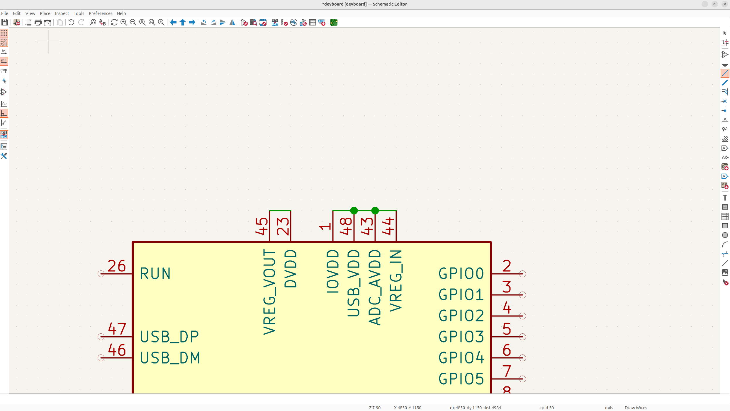
Tap on the "Draw Wires" icon to connect the VREF_VOUT and DVDD, and then separately connect the IO_VDD, USB_VDD, ADC_AVDD and VREG_IN, because these pins have different voltages.
#Add the power symbols
-
Tap "p" to open up the POWER symbol library (you can also tap a, but searching in p will be faster because there's less symbols).
-
Search for "1V1" and "3V3" and place the 1.1V on the VREG_VOUT and DVDD, and 3.3V on the IOVDD and those other pins.
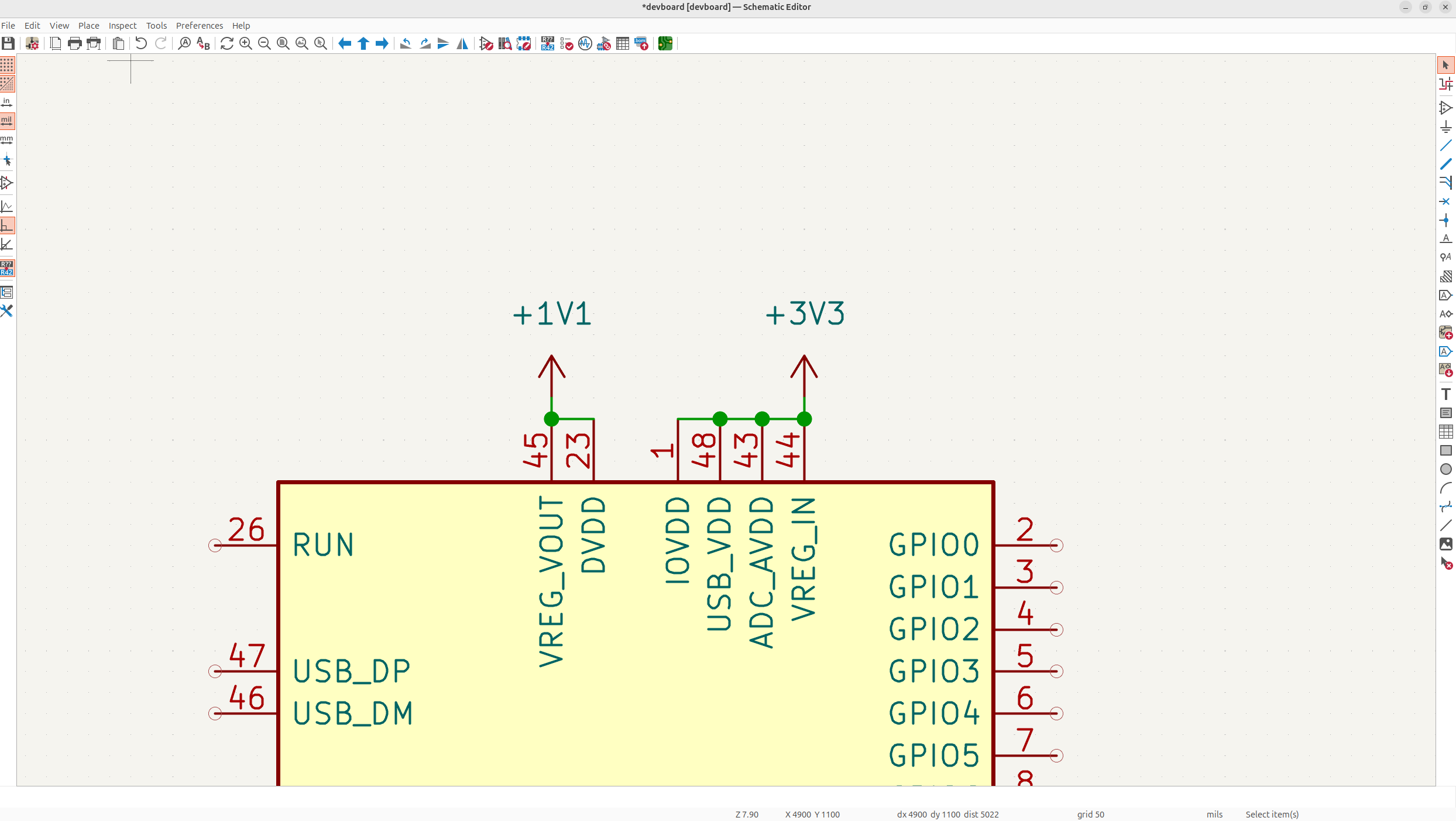
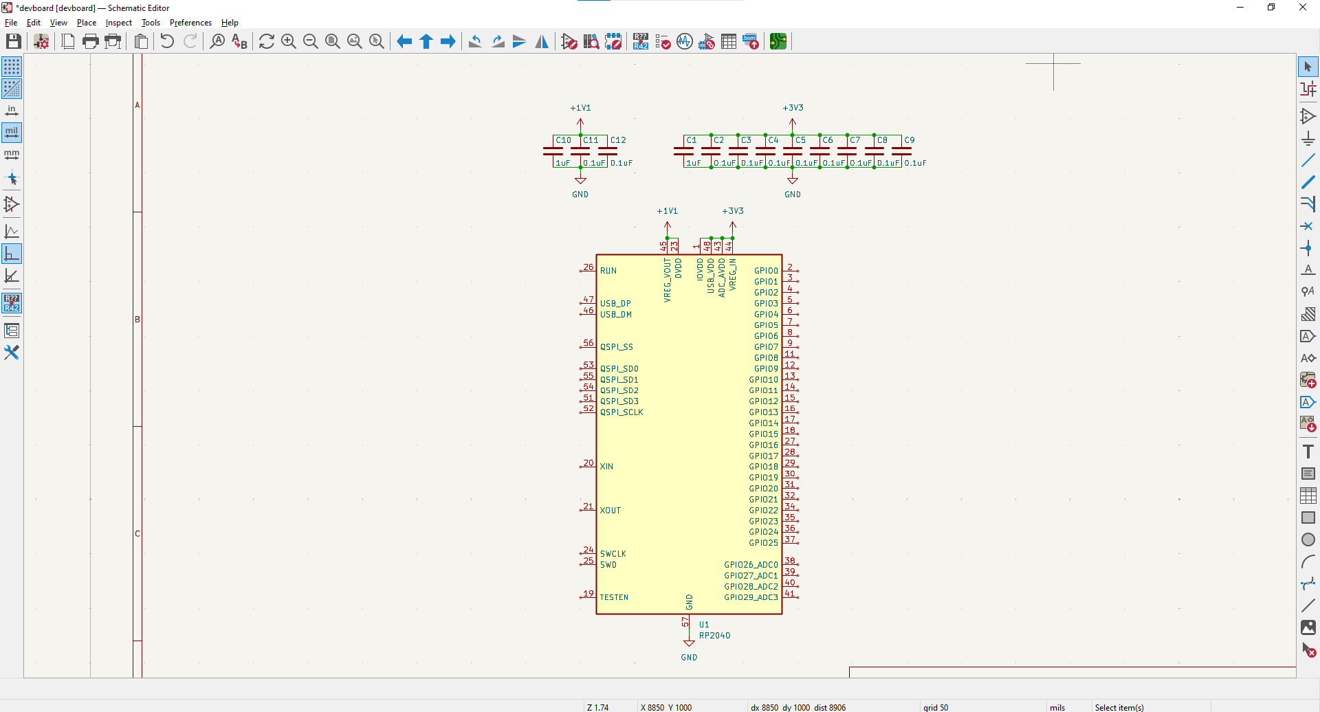
Now that we have our power symbols in, we're going to add the decoupling. You could technically wire them like the screenshot I showed before, but I prefer to separate them because you use less wire which I find looks cleaner, but it's up to personal preference, and readability.
You'll also notice that the symbol contains less pins than the symbol the RP2040 datasheet has, this is because symbols in KiCad tend to not repeat the same pins, so they just merge like all the same VDD pins into one.
#Add the 3.3V decoupling caps
-
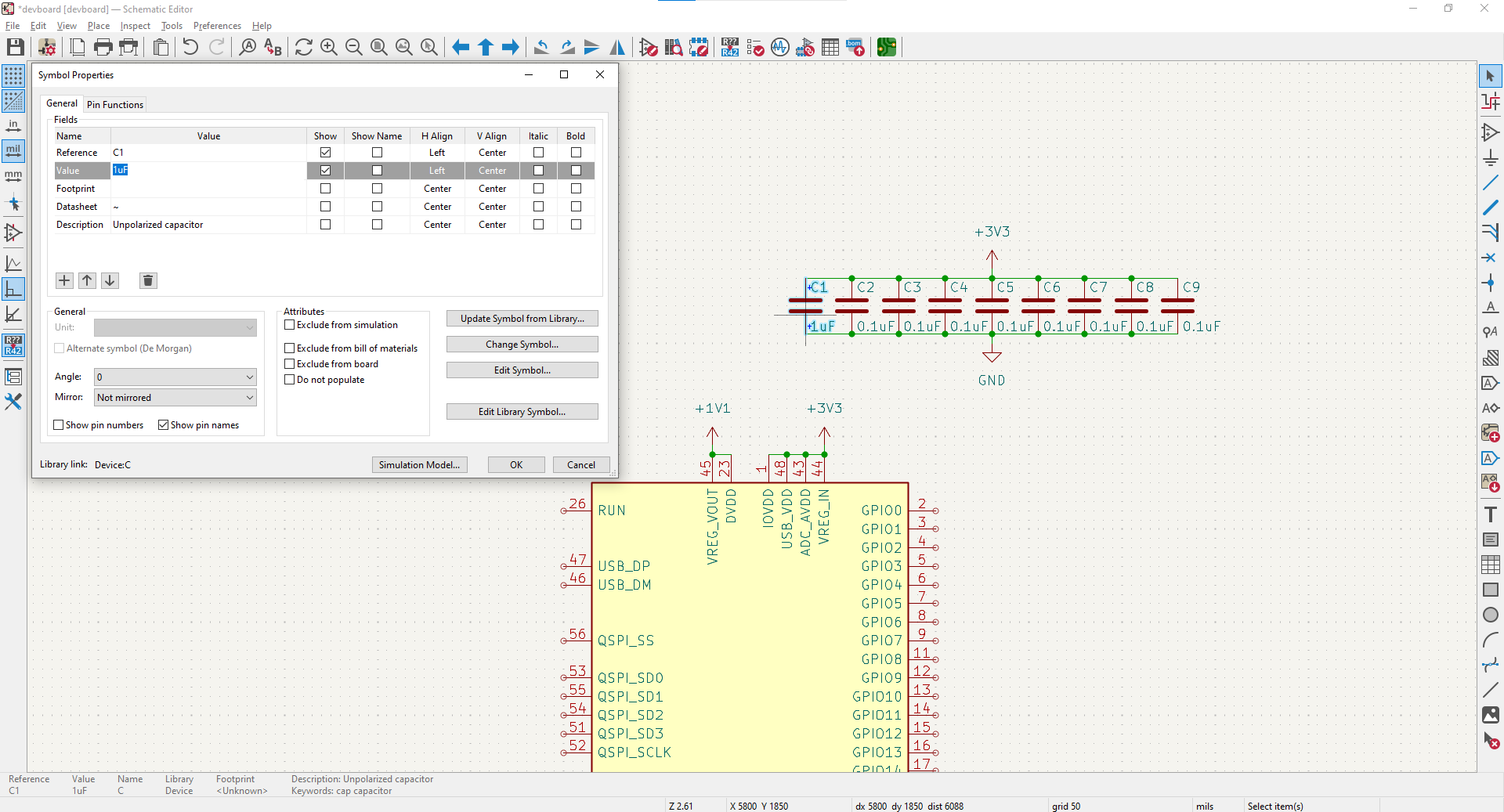
Using the RP2040 datasheet as reference, we know that there's 8 IO VDD pins, so eight 0.1uF decoupling, and one 1uF cap because we're wiring the entire 3.3V line and need to smooth out the larger ripples.
-
Type "a" and search for "c" (the shorthand for capacitor). Make sure to double tap the capacitors to add a value, and make eight of them 0.1uF, and one of them 1uF.
#Add the 1.1V decoupling caps
-
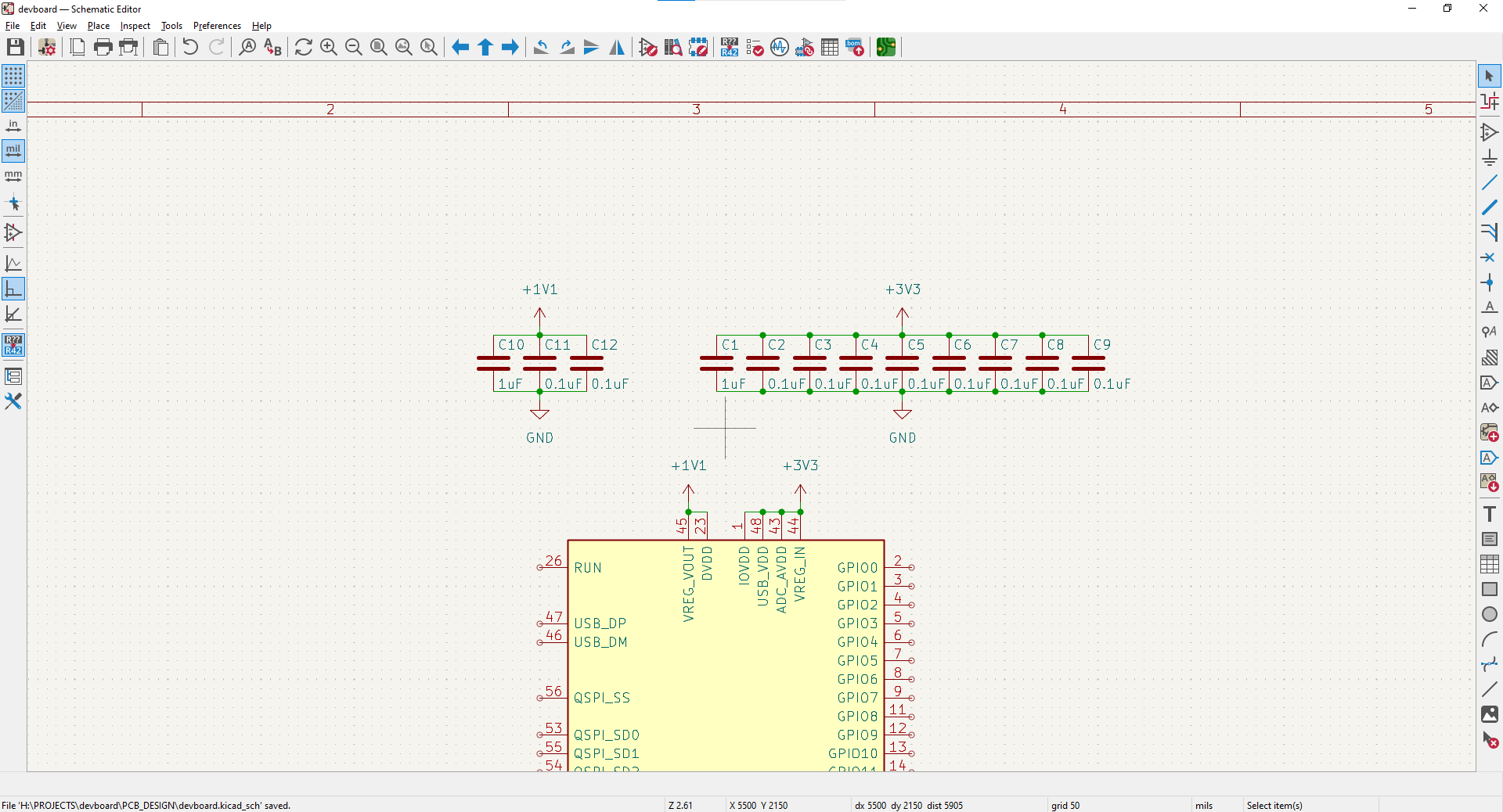
These are the decoupling capacitors for the 3.3V line, now we need to do the caps for the 1.1V line. There's 2 VDD pins, so two, 0.1uF caps, and we need one for the line too, so a 1uF cap aswell:
#Ground the SoC
-
Now we have all of our power decoupling. We also need to connect GND to the SoC, this is pretty self-explanatory, but it allows power to actually flow properly in our PCB.