
Now that we've finished out schematic, we need to start working on the actual PCB. The first thing you need to do for the actual PCB, is to add in all the footprints for your components.
A footprint on a PCB basically just defines it's pads, outline, etc, that your component needs in order to be solder able on a PCB.
#Open the footprint assigner
-
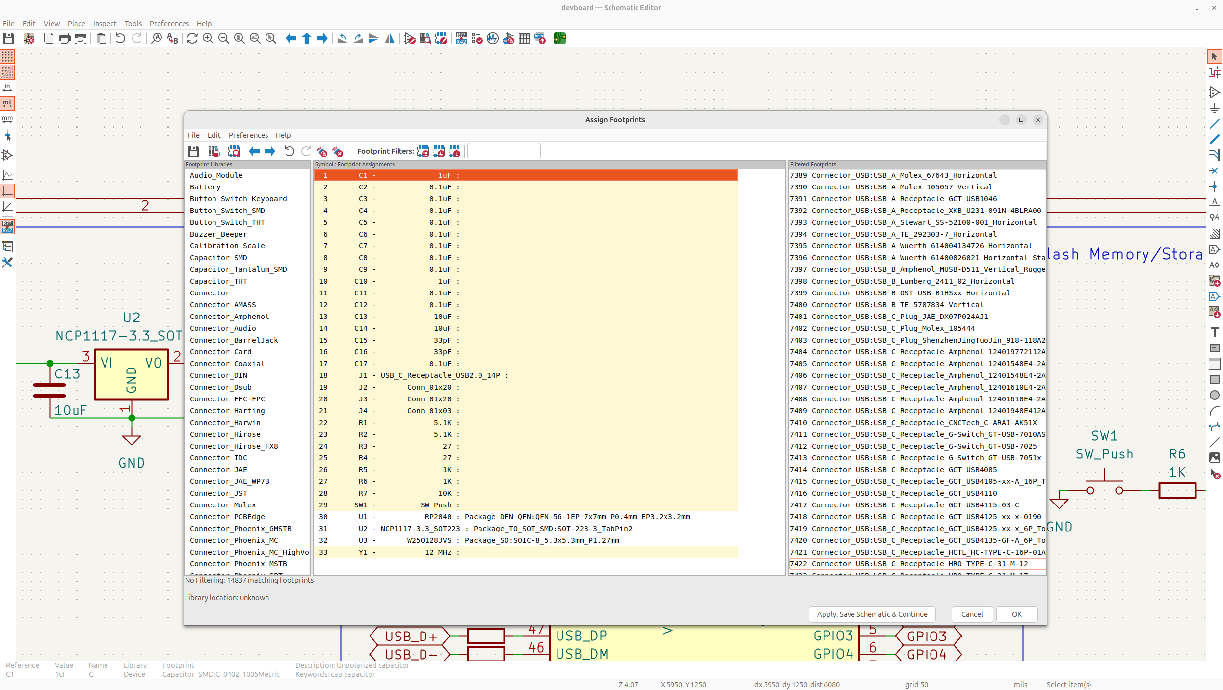
Tap on the assign footprints tab in the top toolbar to open up the footprints tab:
#SMD vs THT
Now before we add in our footprints, let's talk about standard imperial sizes of SMD components, and SMD vs THT components.
So if you don't know, there's SMD components, which are surface mount, which means that the components are attached to the surface of the PCB like caps, and then there's THT components, which are soldered through the board, these are things like the headers.
For SMD footprints, you'll want to understand what the imperial sizes are:
- 0402 are the smallest footprint we'll have on our PCB, these are tiny footprints and anything smaller than this becomes too small to easily solder, these are good for low current applications, and are fine for our fine signal decoupling.
- 0603 footprints are a bit larger than 0402, and are better for slightly higher current and will maintain better physical stability for the larger decoupling needed for 10uF caps and such.
- 0805 footprints are pretty large and are really just needed in higher current applications, we won't be using any of these because we don't have any crazy large caps/components
#Assign passives
-
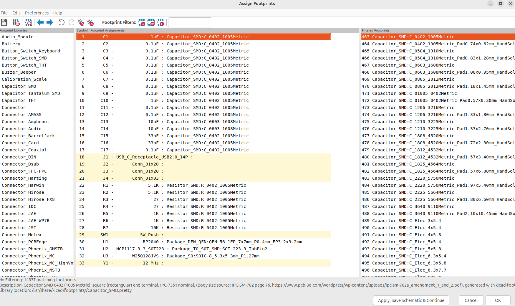
So all of our 0.1uF/1uF/resistors will be 0402, and then the 10uF caps will be 0603, so just filter in the search bar for 0402/0603, and choose the resistor/capacitor footprint for the relative component:
#The rest of the parts
Now these other components need to usually be found on LCSC and then you go into the datasheet to find the footprint, and then add it in, but I'm decently experienced and know what footprints to use already, so you can just copy what ones I'm using or find your own if you want and add them in:
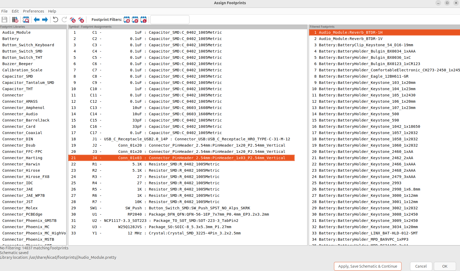
These are my thought process behind the other components, JLCPCB has what's called basic and extended parts, and extended parts cost $3 each to add to a PCB because they have to be loaded into the assembly machines, this will be important here:
- USB_C_Receptacle_HRO_TYPE-C-31-M-12: JLCPCB doesn't have any basic part USB-C receptacles, so I just chose this one I kind of like from a previous board. PART
- PinHeader_1x20_P2.54mm_Vertical: This is just the proper size header pins we need, they should be through hole/THT to be stronger instead of SMD, I mean if you wanted to, it could be SMD though. The part is just pin headers I'll buy separately.
- SW_Push_SPST_NO_Alps_SKRK: This is a small SMD size button footprint found in the JLCPCB basic library, so it doesn't cost anything extra and is pretty compact. This isn't actually the EXACT footprint, but it's close by like .1mm, and I found it by just scrolling through footprints with some filters. PART
- Crystal_SMD_3225-4Pin_3.2x2.5mm: I found this crystal on JLCPCB basic parts, and looked at the datasheet to find the footprint. You really have to make sure your crystal footprint pinout is proper because lots of people accidentally use the wrong footprint or symbol. PART
#Swap the load caps to 33pF
-
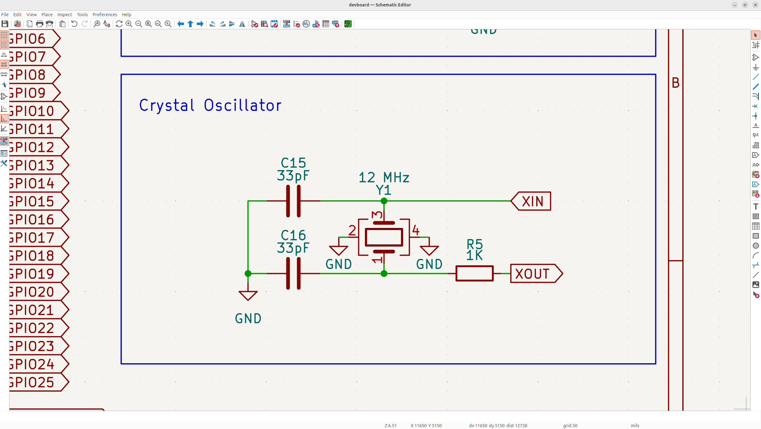
Now we actually need to modify our crystal schematic a bit because of the part we chose on JLCPCB has a load capacitance is slightly different, so we actually need 33pF caps. You can just search up the math if you want to learn how to do this:
And just like that, our schematic and footprint selection is finished, so we can actually get to the real fun stuff.. the PCB!