
Now we have all the components for our board to actually work, so we just need to breakout all the GPIO's on the RP2040, onto header pins so that we can use them in our circuit and whatnot!
#Tie TESTEN to GND
- Before we do this, let's just make sure we attach TESTEN to GND on the RP2040, this pin is just meant for factories to make sure that the RP2040 SoC actually works before sending them out.
#Label the remaining pins
-
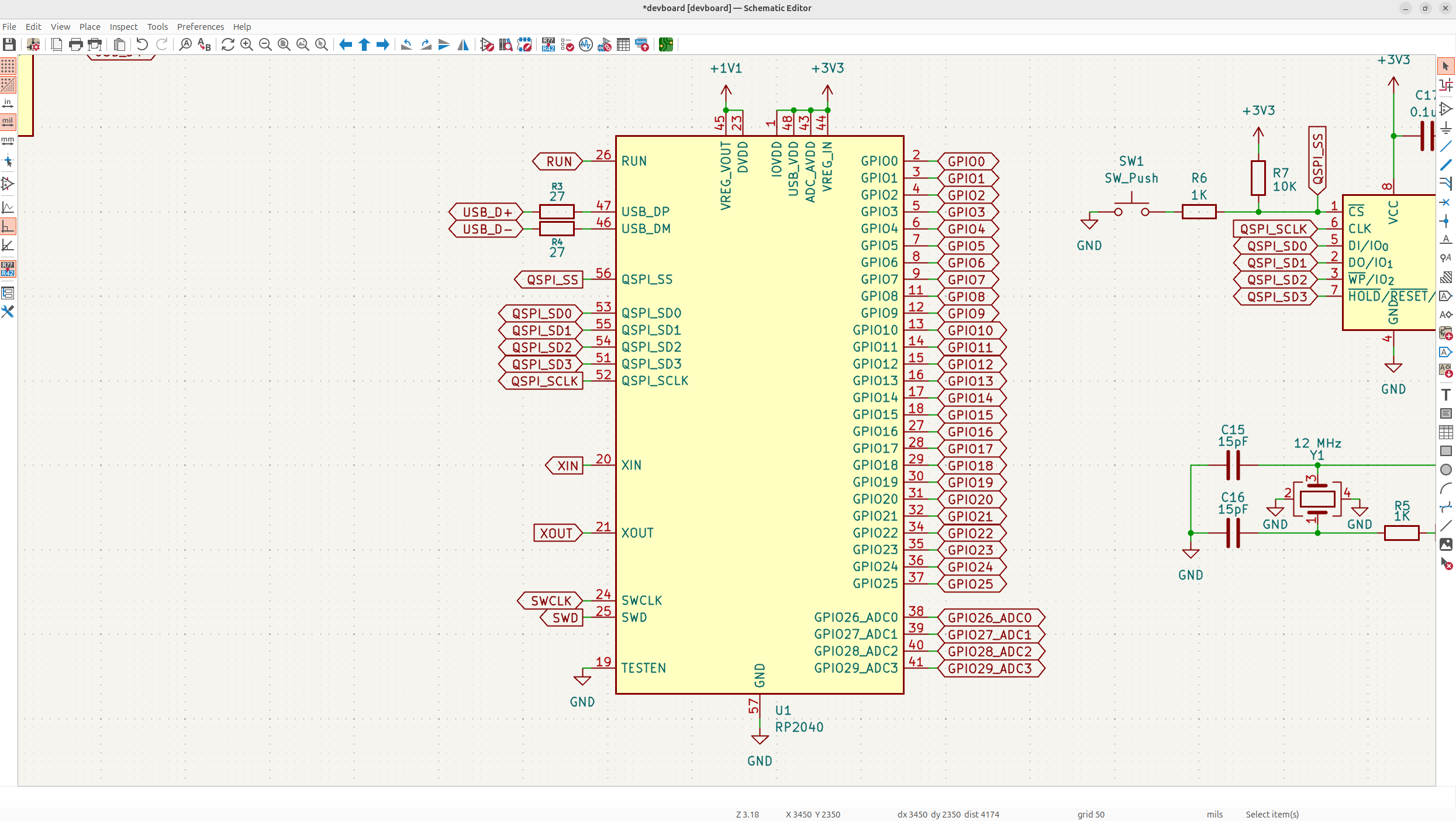
Label all the other pins we haven't broken out (all the GPIO's, SWCLK and SWD), with their relative name on the RP2040. These are all bidirectional pins except the SWCLK pin, which is a clock output from the SoC:
-
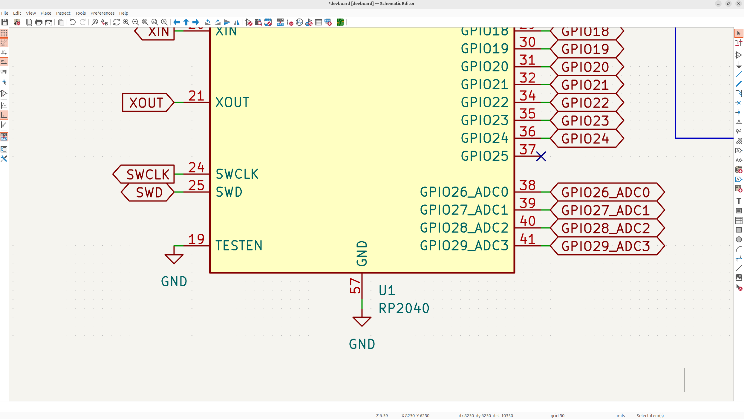
I actually labelled mine the wrong direction for the rest of this tutorial, but it's purely cosmetic and won't actually impact my PCB, this is how it should actually look, don't mind the GPIO labels, I took this screenshot after being done the PCB:
#Add the header symbols
-
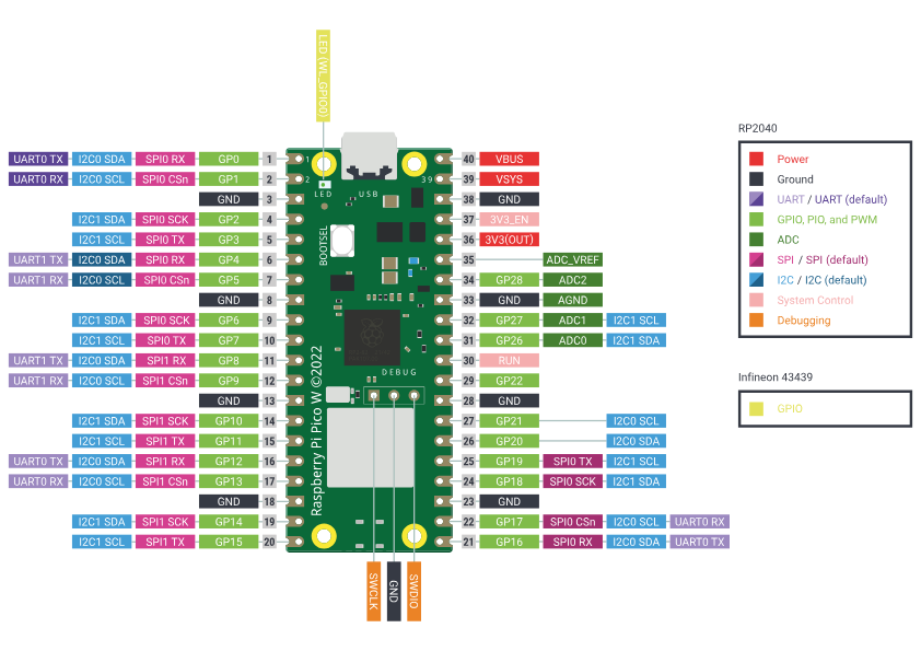
Next, we're going to add the actual header pin symbols into our schematic. You can technically do this whoever you want, but I'm going to adhere to the raspberry Pi Pico pinout:
-
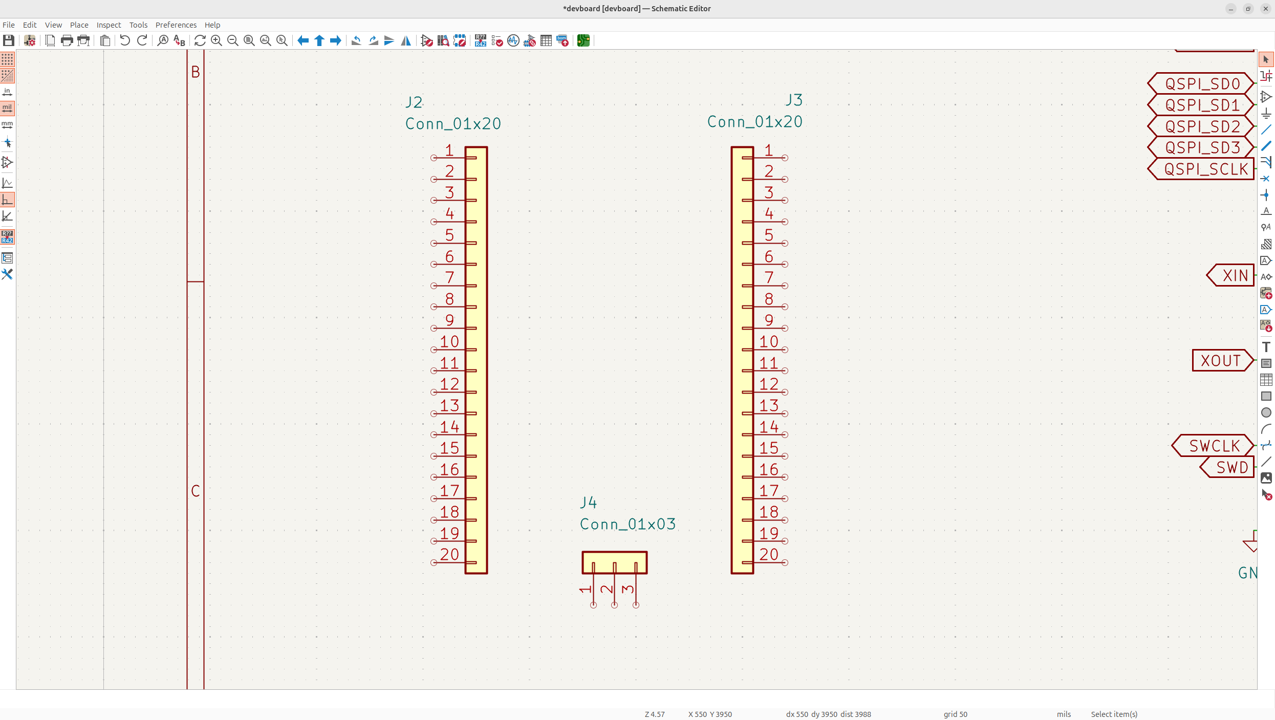
So add in a two, 1x20 header pin symbols, and one 1x3 header pin symbol, I just used generic symbols, but you could use pin header symbols if you want, it's just up to preference:
-
Usually you don't want to make your symbol layout look exactly like your PCB, but I think it makes it more obvious so that we don't mess up our pinout!
#Wire up the pins we know
-
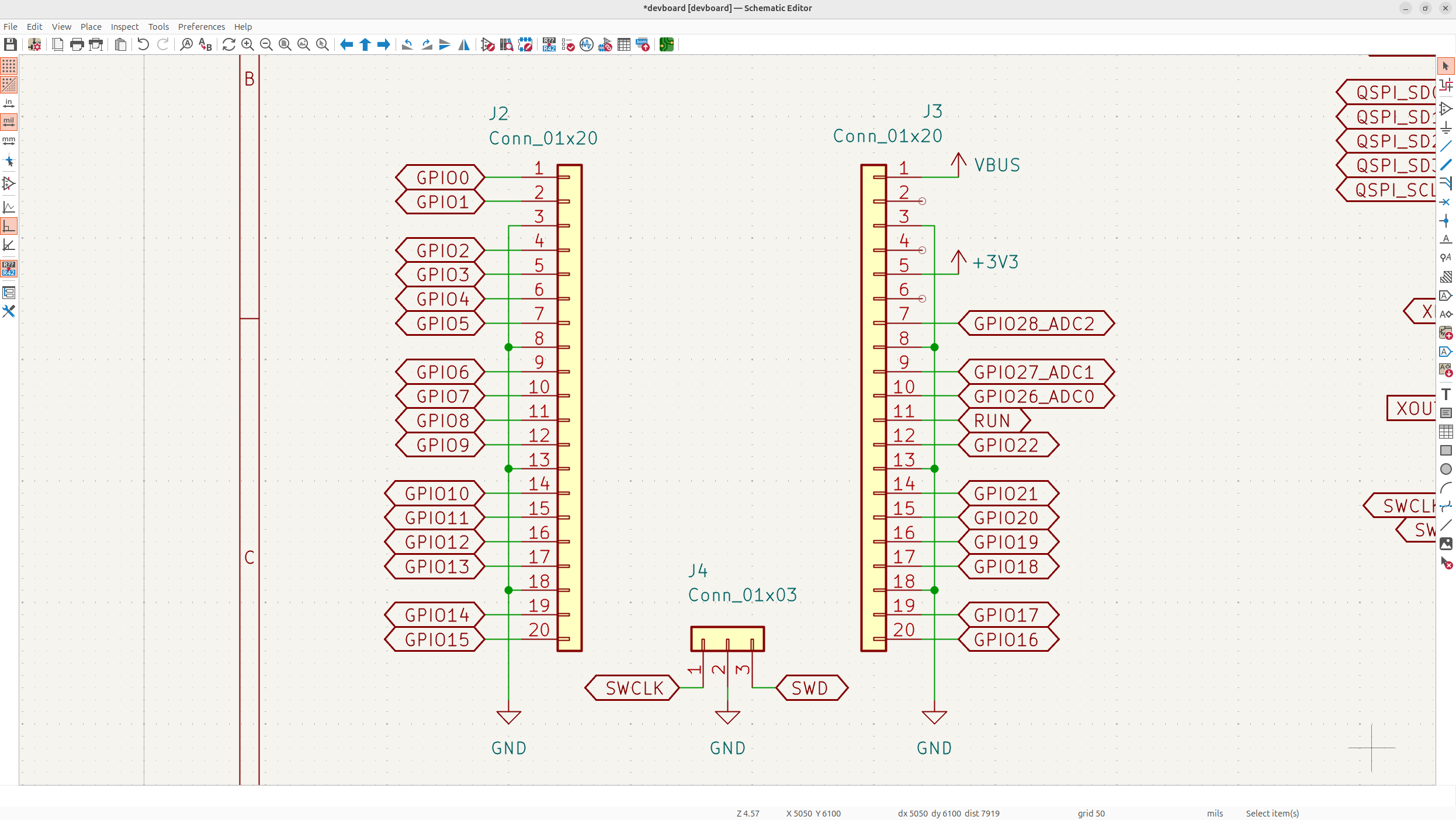
Add in all the pins, and we'll just leave out the ones we don't know yet like VSYS, 3V3_EN and ADC_VREF, I'll explain those after:
#The pins we skipped
Now the Pi Pico can actually be powered by a battery, but we're not implementing a battery (if you want to, check out the Pi Pico datasheet), so there's a diode on the VBUS power line, so they have a VSYS line after the diode and a VBUS line before it, but because we don't need a diode, we don't need VSYS.
We also don't need 3V3_EN, and then ADC_VREF is kind of just another thing to give a reference voltage to ADC, but it isn't really necessary, and we're just making a simple devboard so we won't use it.
#Fill the free pins with GPIOs
-
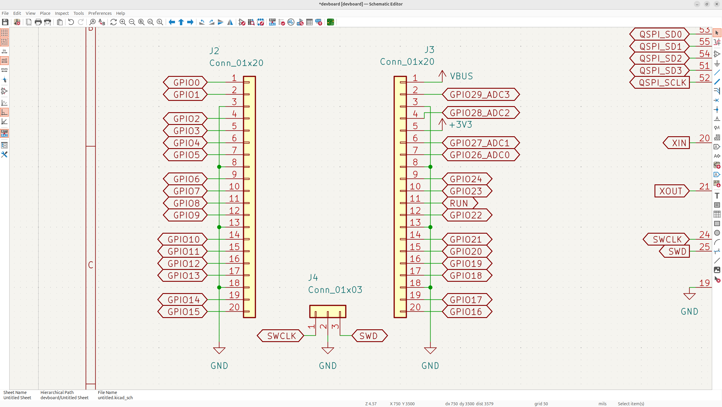
Because we have these free pins, and also some GPIO's still left, let's just fill these pins with some GPIO's. I'm going to move the ADC pins up, and then fill the other pins with GPIO's. I also want to use GPIO29 which is an ADC pin and replace GPIO25 with that just so we get the added ADC pin:
#No-connect GPIO25
-
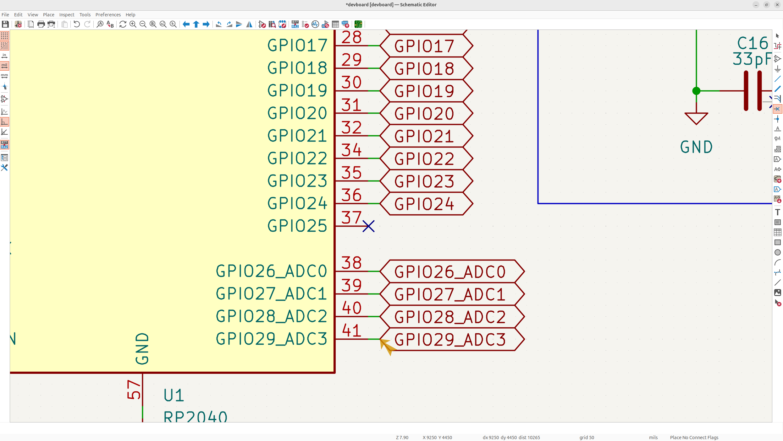
Because of this, you'll want to just no-connect GPIO25 on the MCU, just to tell KiCad and others that we're not using that pin:
If you want to add battery support, you can do so yourself, but I'm keeping to a minimum framework. And just like that, we have all of our header pins in!
#Finishing up the schematic
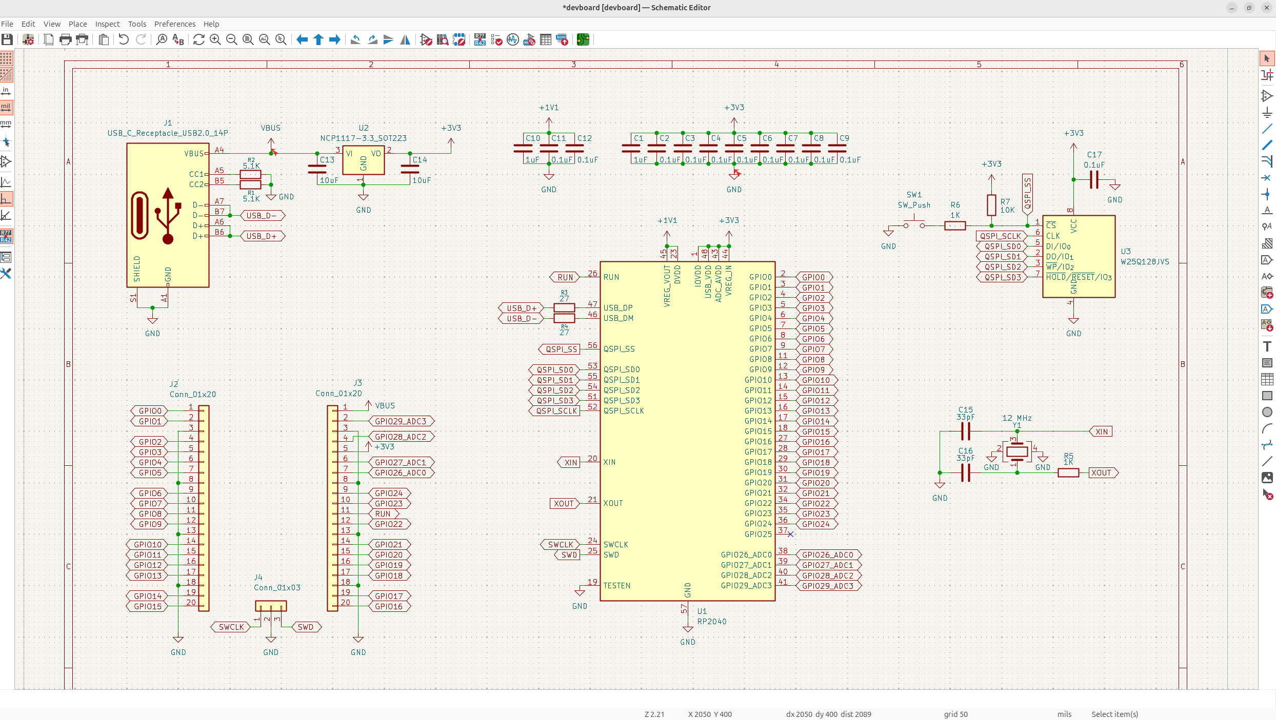
Now that we have our I/O headers in, we're actually finished with all the symbols in our schematic, this is how your schematic should look:
#Group the blocks visually
-
Now to organize our schematic, even more, let's separate our design into different blocks using the text boxes in the schematic editor. When doing this, you usually want to place your component blocks by flow of your PCB. So if you could image, power flows in through the USB, so we'll put that in the corner, the MCU should be center because it's the fundamental of the PCB, and then the other stuff can just be organized around:
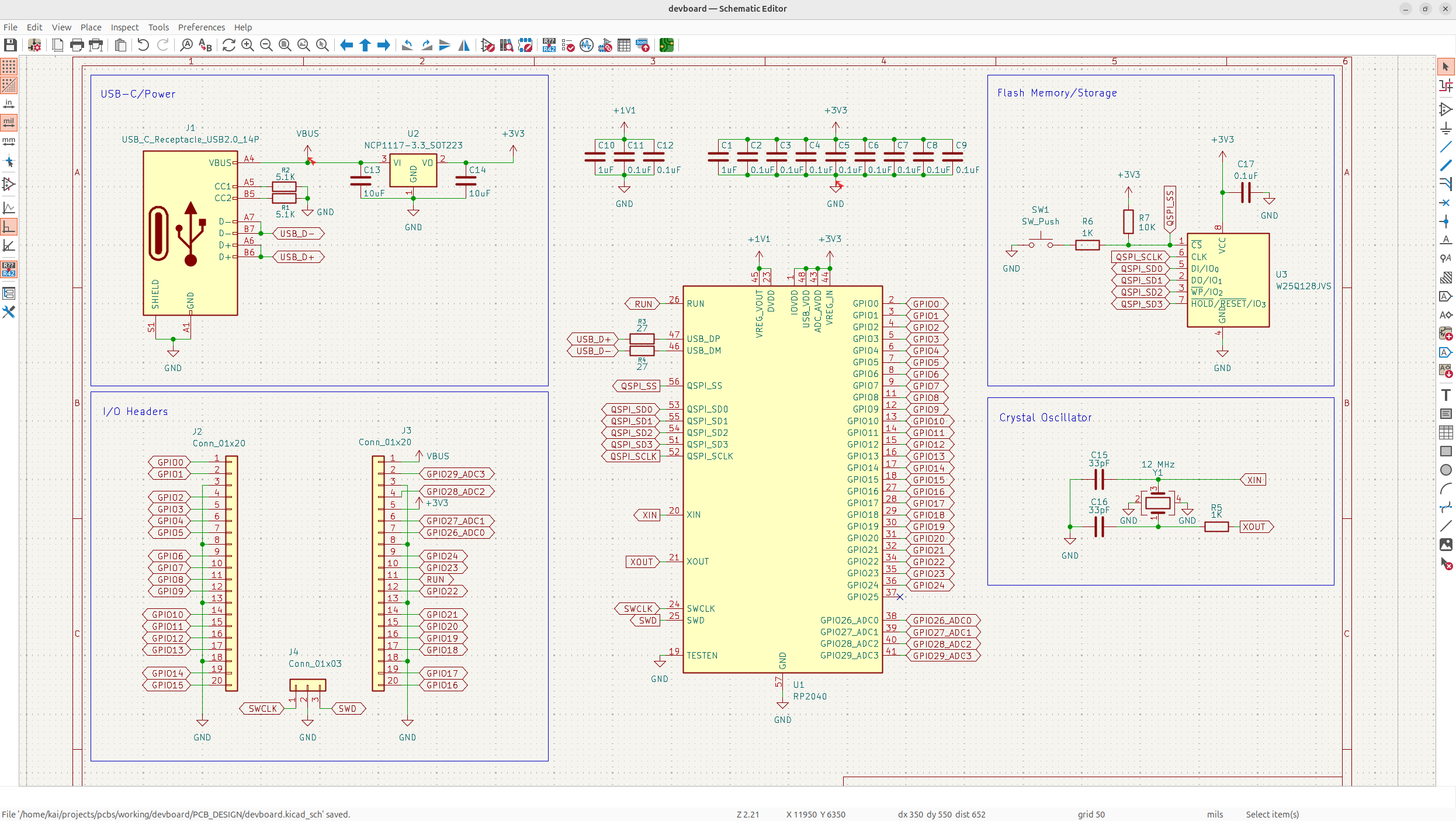
-
You don't have to do this, but I feel like it keeps everything nice and clean!