
Now lot's of SoC's include flash storage, but the RP2040 actually doesn't, so we need to add on our own flash storage! You can think of flash storage as like a faster version of an HDD, with less power consumption, more reliability but is usually a bit more expensive.
Sadly, the RP2040 only supports up to 16mb of memory, so we'll just use a quad SPI flash memory IC (integrated circuit, those little chips on a board) like the W25Q128JVS used in the datasheet.
#What is SPI?
Now before we actually add it to our schematic, let's talk about what SPI is. If you continue to build PCB's, you'll see this communication interface very often, it's basically just a standardized way of transferring data. The signal comes out of the master, and then goes into slave devices. The master is our MCU in this case, and the slave, is our flash memory.
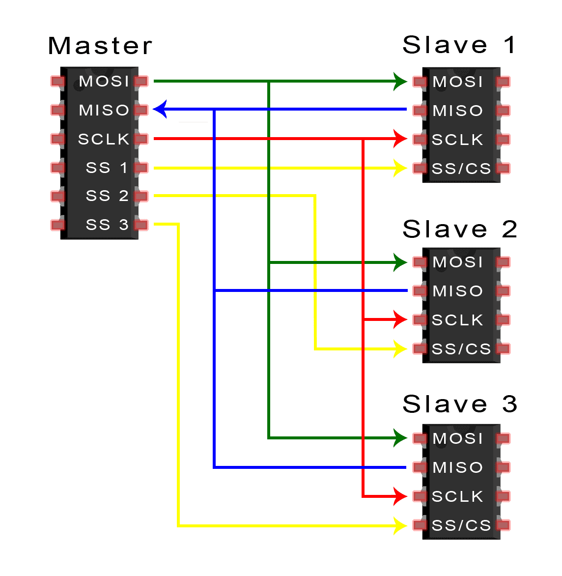
It has 4 major pins you need to understand:
- MOSI - Master output, slave input
- MISO - Master input, slave output
- SCLK - Clock signal (remember that oscillator we added to our board, this will basically do that for other devices)
- SS/CS - Slave select, let's you choose what device you're communicating with
So you usually need to have all 4 of those, and then you can add SS pins as you wish if you want to communicate with more and more devices.
But we're actually using quad SPI in this case.
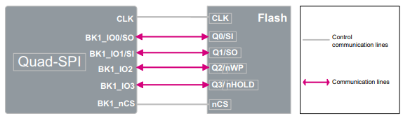
Quad SPI uses the same CLK and CS pin, but has 4 IO pins, so it can transfer data, 4x as fast as SPI, which is ideal for flash memory, but it does take up more pins, so that's why it's not always used.
Now you can't just attach SPI to any GPIO, you have to use what's called a hardware controller, which you can imagine, is like a little block on the RP2040 SoC that is specifically meant for SPI. There are 2 SPI controllers on the RP2040, so we're going to use them for our flash memory. You can also technically do SPI via software, but it just makes way more sense to use the actual controller provided.
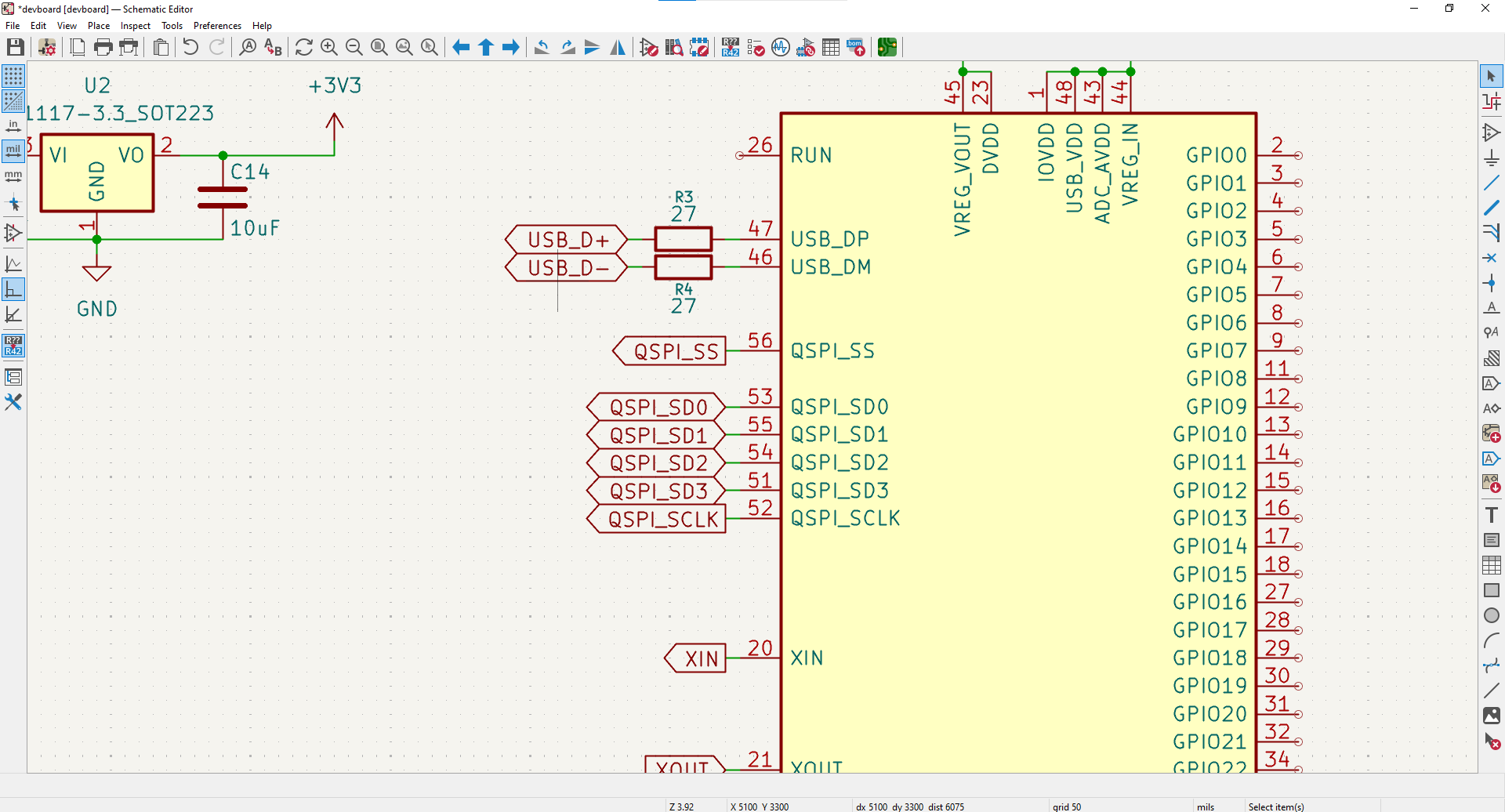
#Label the QSPI pins
-
Add a global label to the QSPI pins with their relative name, IO's are bidirectional, and CLK and CS/SS are inputs to the slave (the flash memory) or outputs from the MCU.
#Wire the flash IC
-
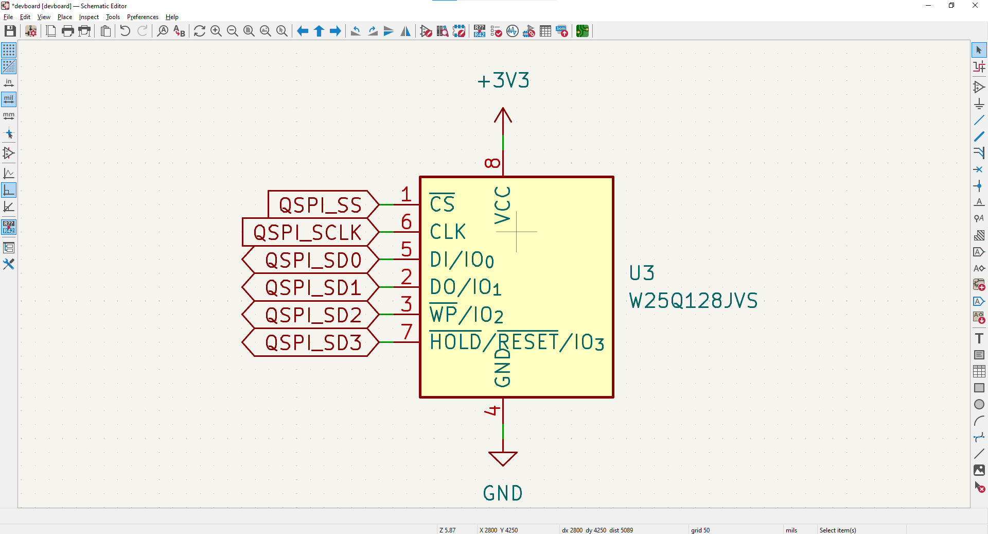
Add in our flash memory IC (chip), W25Q128JVS, and wire up all the QSPI pins, and put GND to GND, and VCC to 3.3V:
#The BOOTSEL button
Next, we need to add our 100nF/0.1uF decoupling capacitor to our VCC line to filter high-frequency noise. And then, we're going to add a button to the CS line, so that we can enter what's called BOOTSEL mode.
Based off of the RP2040 datasheet, if the QSPI SS pin, see's a 0 or GND when it's booting up, it'll go into BOOTSEL, where it will appear as a USB device on our computer so that we can copy code onto it to set it up.
#Add the BOOTSEL button + resistors
-
Wire in the decoupling cap, the BOOTSEL button on the CS line, a 10K pullup to 3.3V, and a 1K resistor in series with the button.
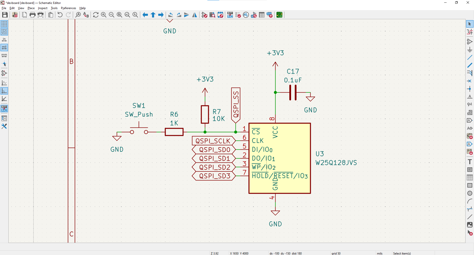
Now there's 2 resistors you're probably wondering about here, the pullup to 3.3V, and the one in series with the button.
The pullup to 3.3V is important, because usually the QSPI pin will show up as 3.3V to the flash memory, but during bootup, you can't guarantee that it will, because the pin isn't active, so you might have some weird thing that happens with your board. The 10K resistor is just standard that the RP2040 datasheet wants us to use (and is also pretty commonly used to filter noise and stuff). If pull resistors are still fuzzy, read Pull-up Resistors before continuing.
The 1K resistor in series limits the amount of current that can flow in this part of the circuit to prevent damage to the CS pin.
And just like that, we have our button and decoupling in, and our flash memory is completed!