
Now that all that stuffs done, tap the switch to PCB editor button on the far right of the top toolbar!
This will bring you into a new editor you haven't seen yet, this is where we'll actually place down the components on our PCB, and route everything.
#Pull components in from the schematic
-
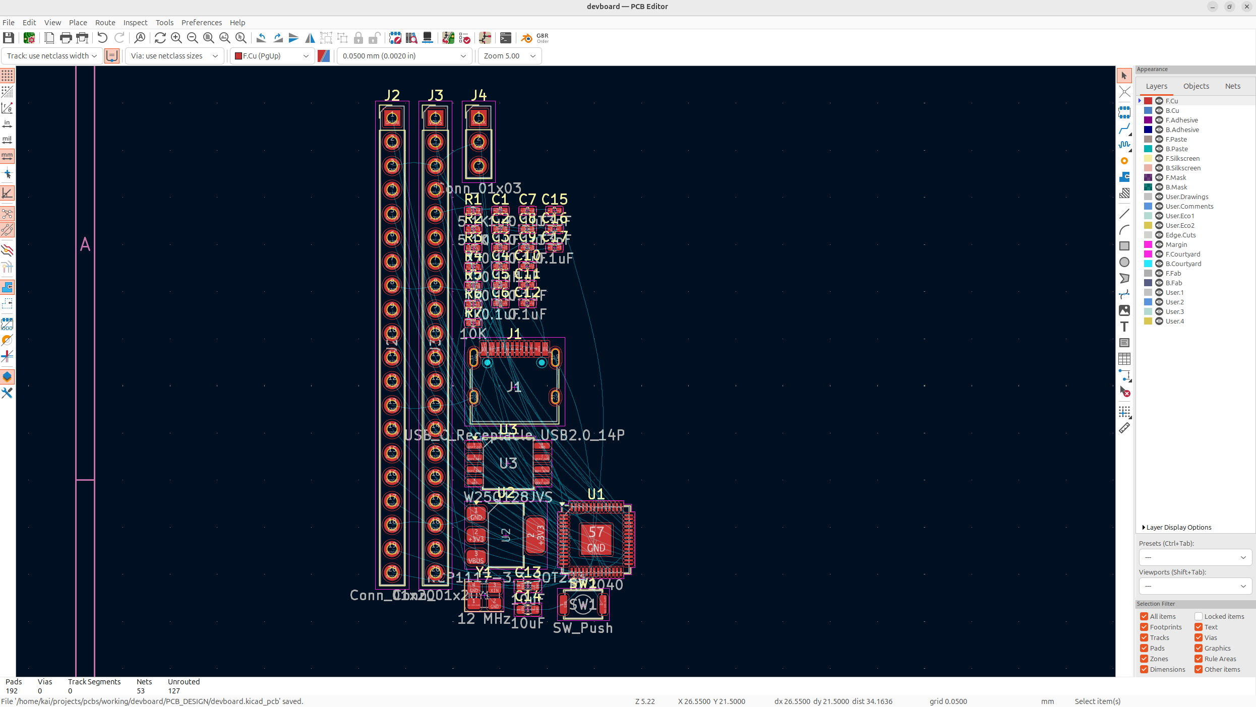
In the top toolbar, tap the update PCB from schematic or F8, and then tap the update PCB button that shows up, to bring in all the components into your PCB, and just put them all in the top left corner of your PCB:
-
You might get some warnings which can be ignored usually (I just got some pin warnings which are fine), but there shouldn't be any errors.
-
Now you'll see our actual components on the PCB, our USB-C, the RP2040, the button, crystal, LDO, flash, headers and our caps/resistors!
#Board outline & positioning
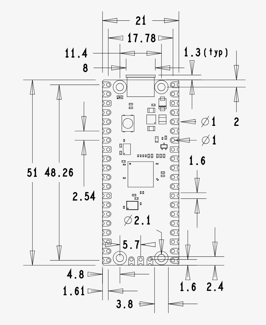
Now before we actually lay out all of our components, we need to define our PCB outline, holes, etc. So using the datasheet as a reference, we'll place down everything accordingly. Start with the board outline, and then do holes and stuff.
#Draw the board outline
-
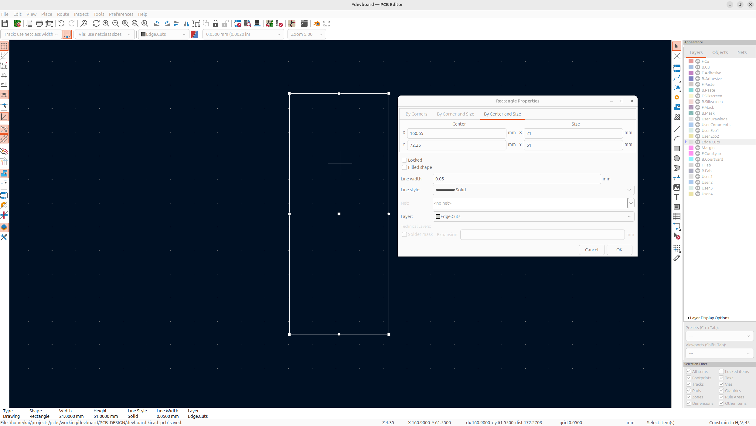
To add in a board outline, tap on the Edge.Cuts layer and then tap on Draw Rectangles, and then just put whatever size rectangle you want.
-
After that, we'll add in the proper size from the datasheet, which is 21x51mm, so tap on the rectangle, then tap "e" and use the By Center and Size tab to do this:
#Align the top header pins
-
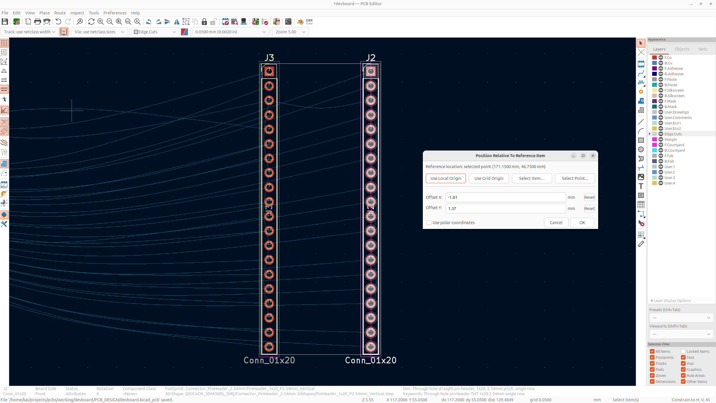
Align the header pins onto our PCB by using the position tool. So right click on one of the header pins, go Positioning Tools → Position Relative To, and then go Select Point and tap one of the top corners of the board outline.
-
Using the datasheet, align the X to 1.61/-1.61 based off of the side, and the Y to 1.37:
-
(I actually swapped my pin headers here which I fix later, but just put J2 as the first header, and J3 as the second one, so it's easier to route)
#Align the bottom header
-
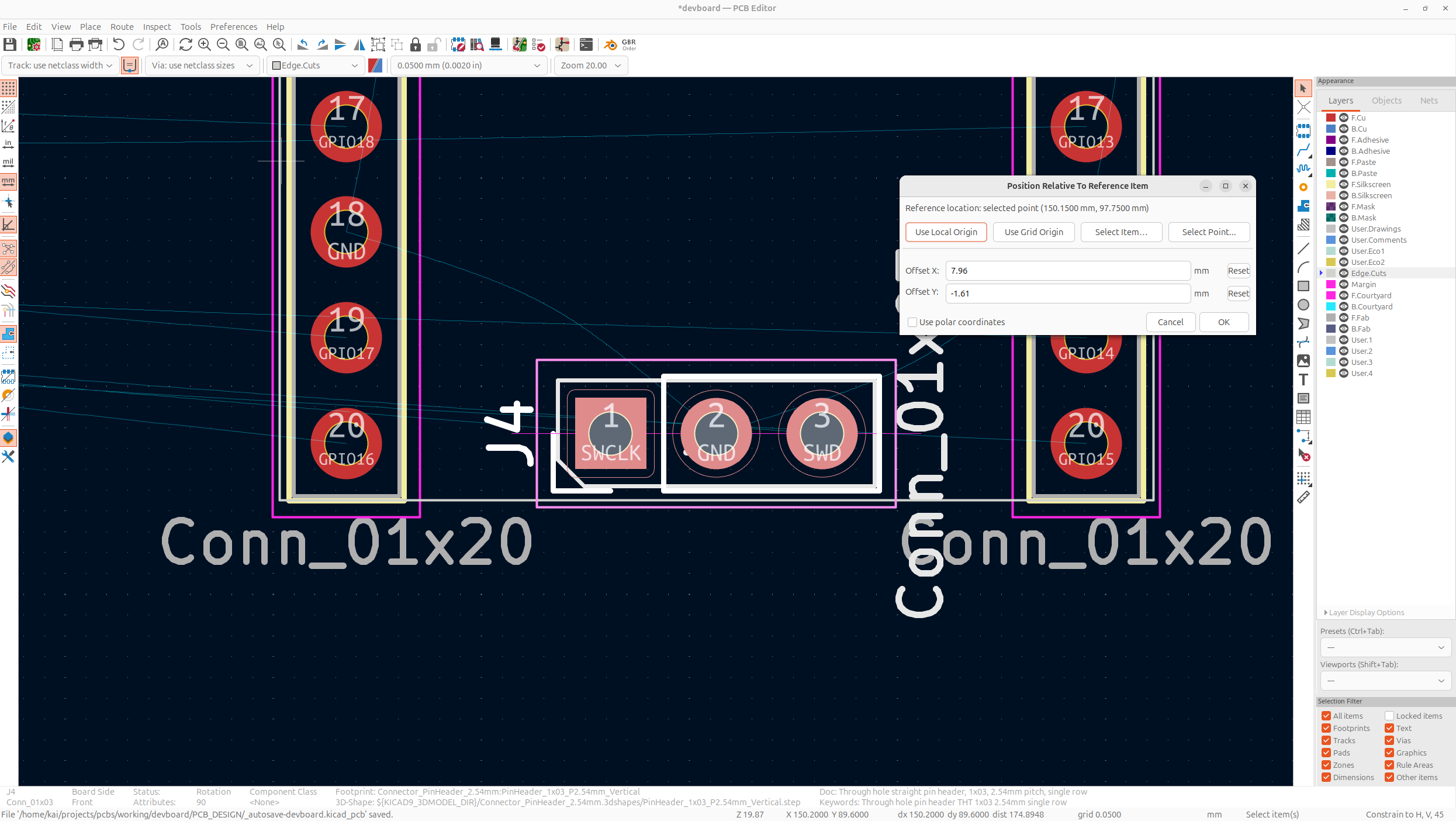
Put our bottom header in, these are aligned to Y -1.61 and the X should be centered so 7.96 (10.5 is the center, minus 2.54 the pin spacing), and use the bottom left/right as reference (make sure it's flipped horizontally when aligning):
#Center the RP2040
-
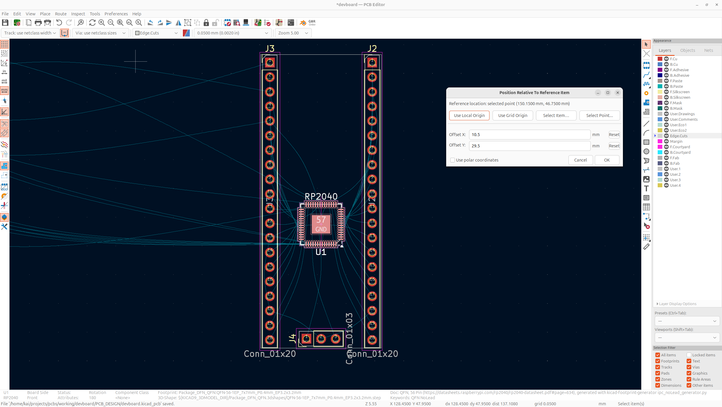
I'm going to put in the RP2040 dead center, but with the Y slightly farther down, because there's more components above the Pico than below, so I want a bit more space for signals, I'm going to put it down an extra 4mm, but you can do how much you want.
#Center the USB-C
-
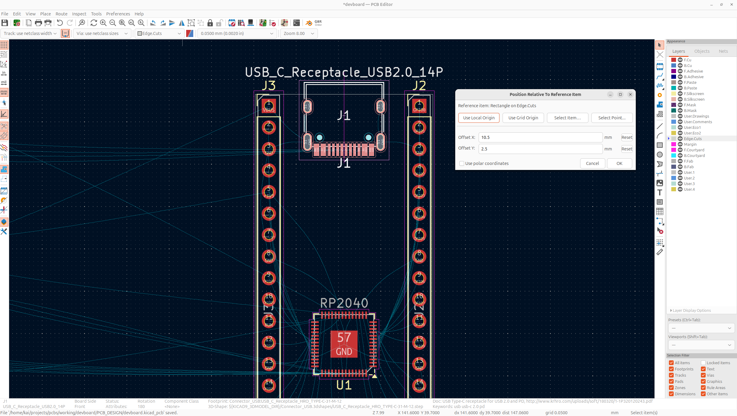
Center the USB-C, down a bit to the top of the devboard:
#Smaller footprints for LDO & flash
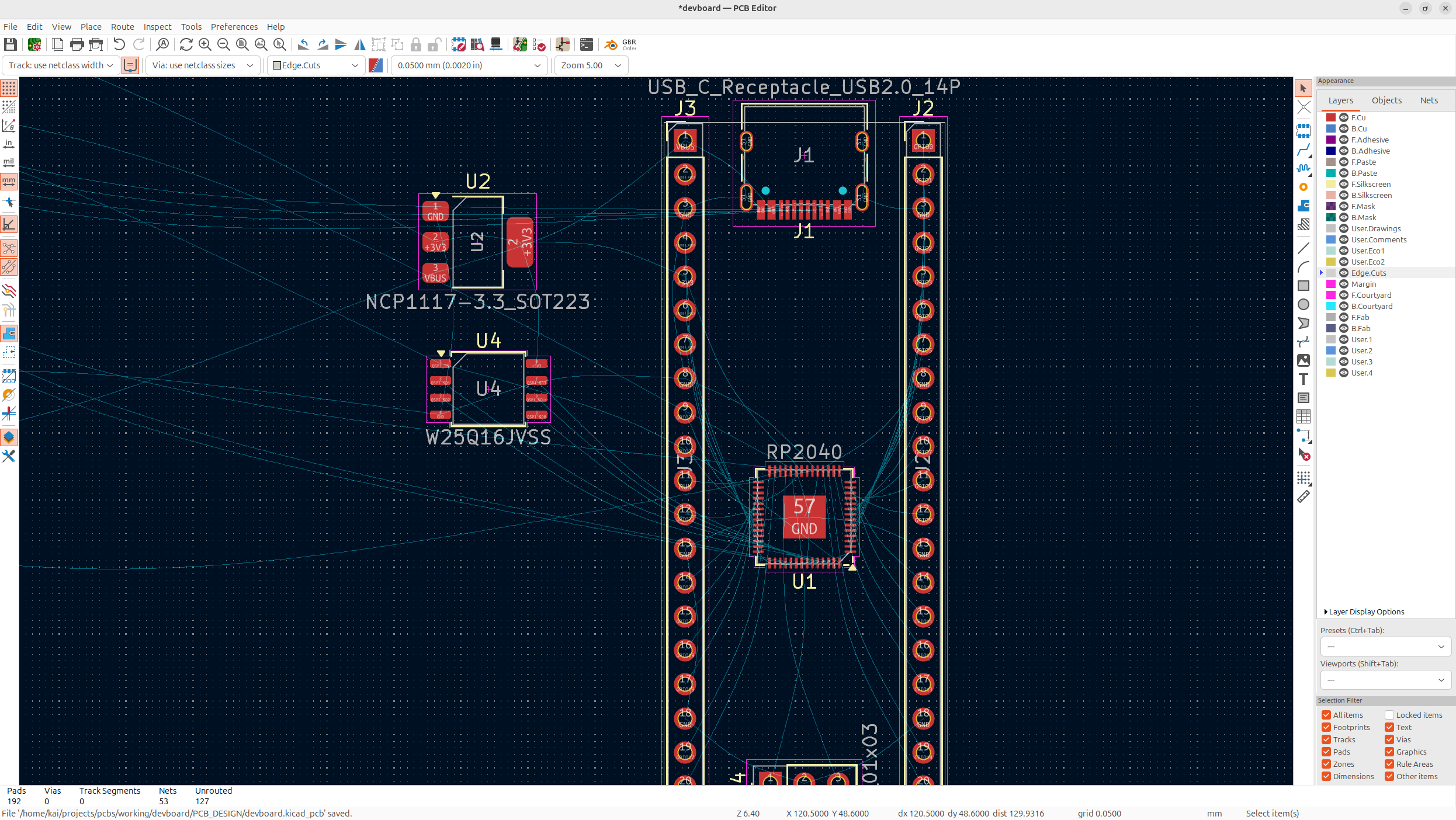
Now looking at the flash memory and LDO IC, they're really big, so let's use different components for them:
#Swap the LDO to MCP1700
-
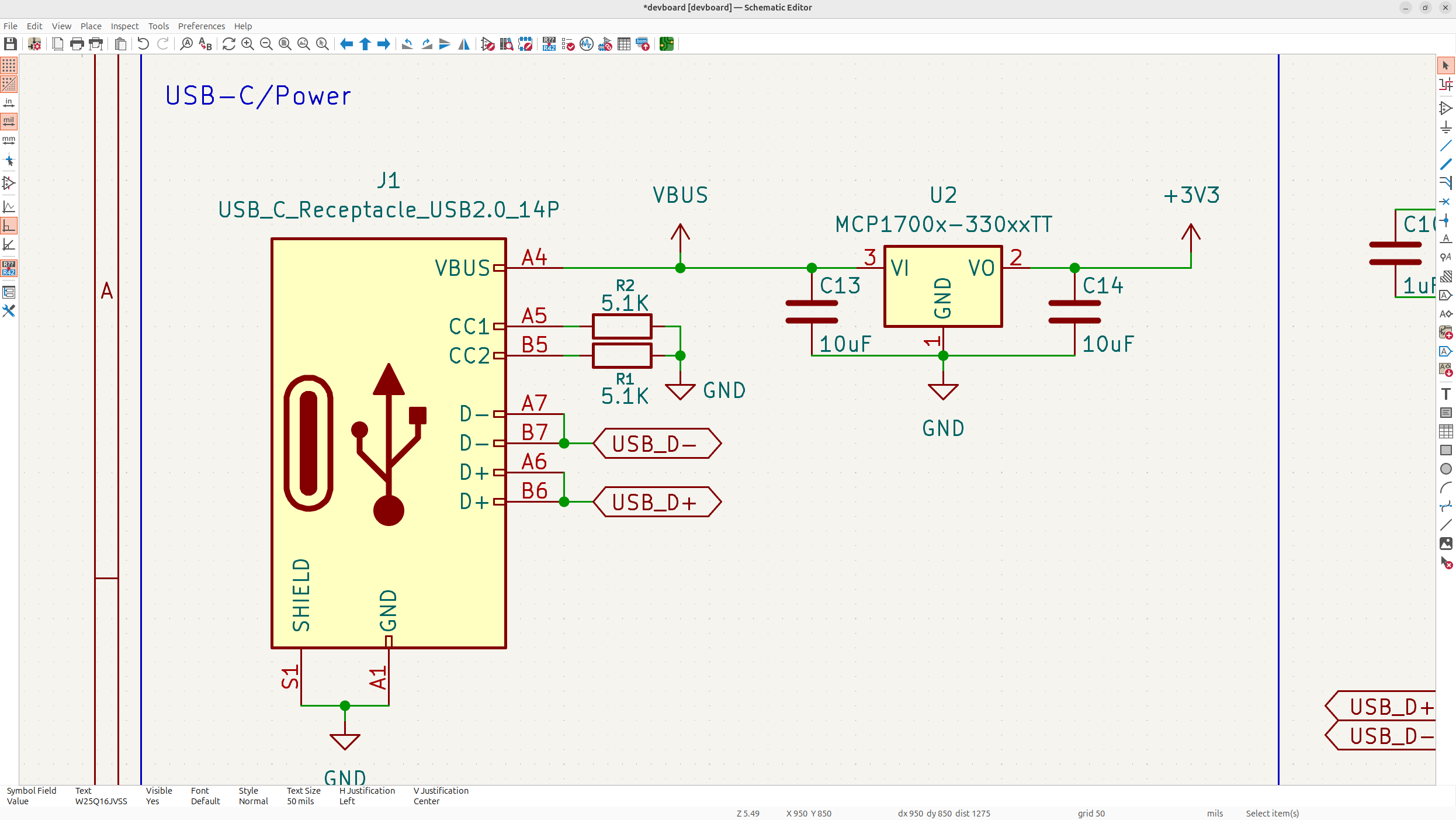
I'm going to switch to the MCP1700 LDO, which is smaller, but does handle less current (250ma), so if you plan on drawing more current, you might want to just keep the current LDO. So just replace the NCP1700 with the MCP1700x-330xxTT, which is the 3.3V MCP1700:
#Swap the flash to the Pi Pico one
-
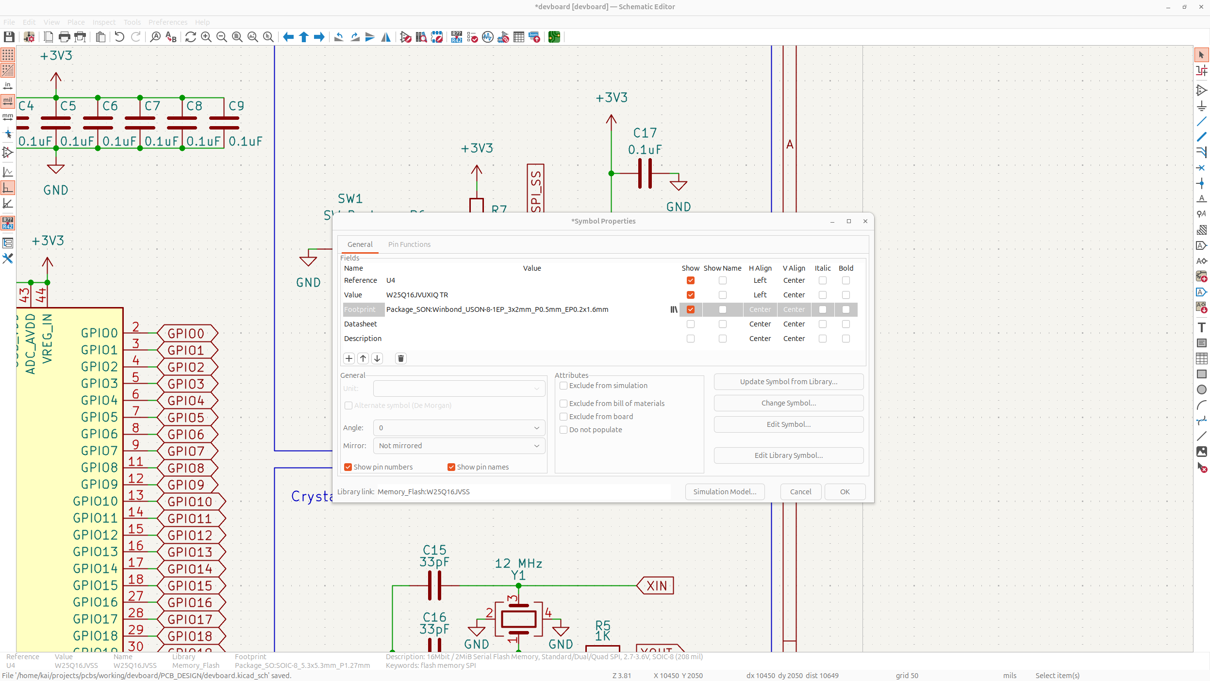
Change the flash memory to what the Pi Pico uses and has a slightly smaller package, which is the W25Q16JVZPIQ TR and uses the Package_SON:Winbond_USON-8-1EP_3x2mm_P0.5mm_EP0.2x1.6mm footprint, so switch the footprint to that new one!
-
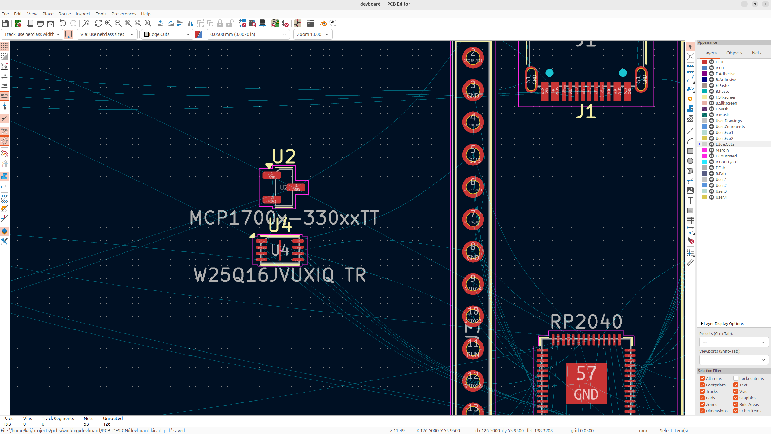
Now your footprints should be much better:
#Placing components
#Group the parts by flow
-
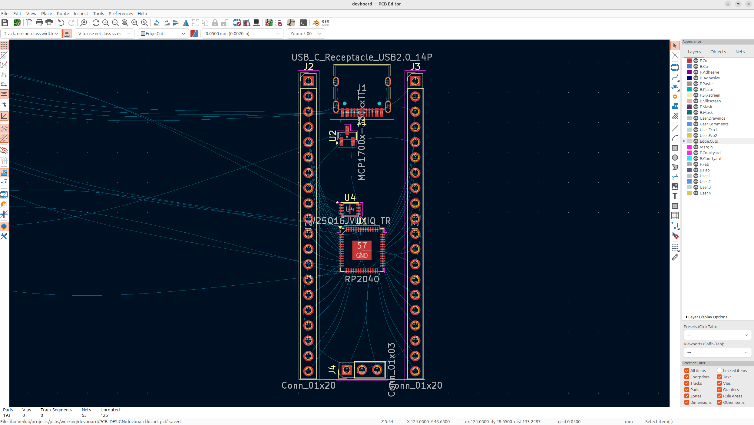
We're going to organize our parts onto the PCB (I also fixed my header pins and MCU orientation in this step). The LDO is going to go really close to the USB-C VBUS, and the flash storage will go close to the RP2040's QSPI pins, just so we have an efficient layout:
-
I use exact positioning when doing things like this, but you can just place them on if you want, I just like everything to be nicely symmetrical.
#Place the crystal close to XIN/XOUT
-
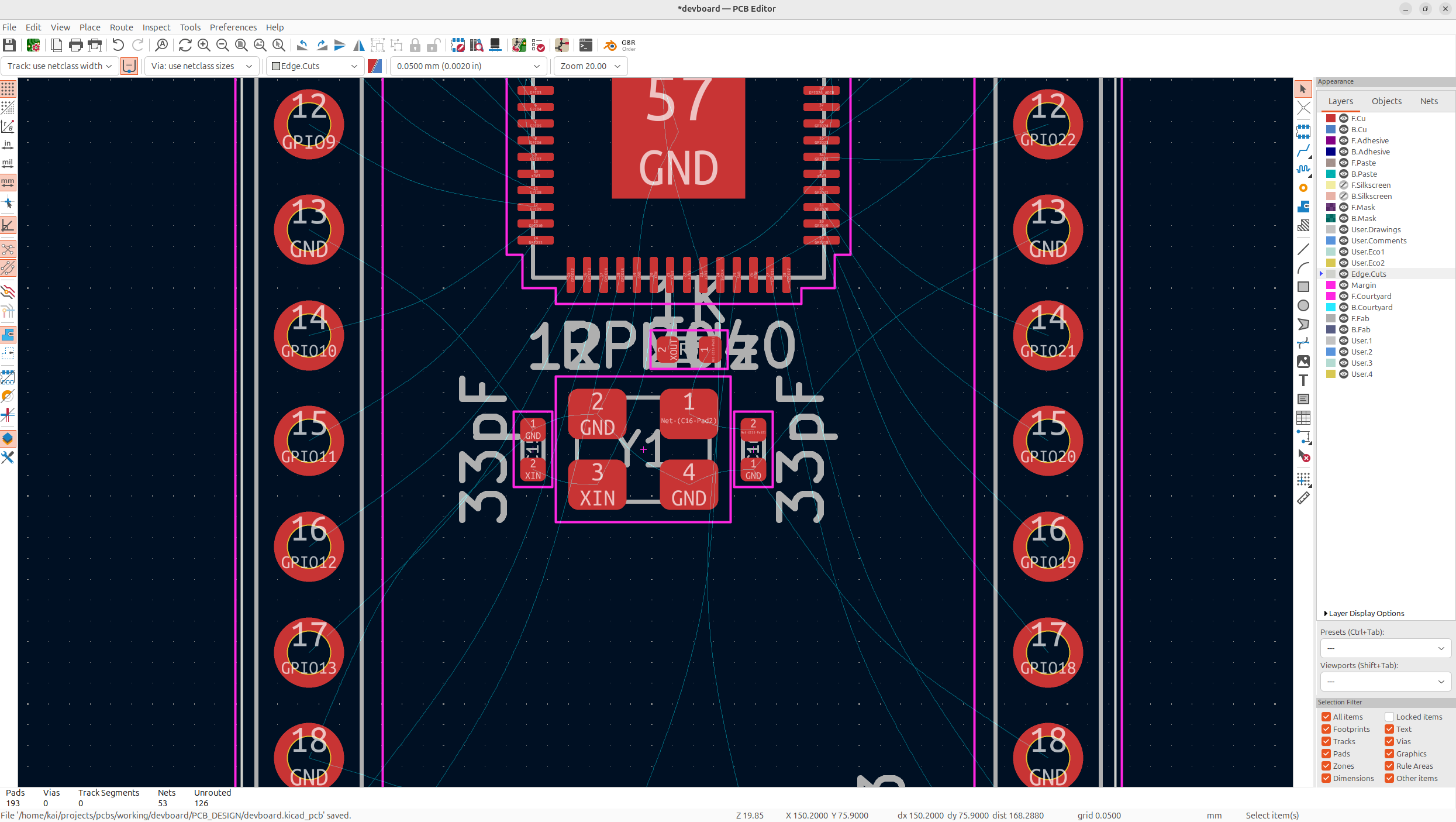
Put the crystal on. The crystal should be very close to the RP2040 XIN/XOUT pins because it's a very precise signal, and the load capacitors should be RIGHT next to the pins too so the signals don't get messed up. You can then just put the resistor right by the XOUT pin of the RP2040 to have a nice and efficient layout:
#Place the decoupling caps
-
Put all the decoupling capacitors on my board. Decoupling capacitors should be as close as possible to the pins they're decoupling, the larger the cap is, the farther it can be, but try to keep them close to their pins.
-
Also feel free to mess with layout a bit during this step just so everything fits in efficiently! Try to use whatever capacitor you used in your schematic for organization purposes.
-
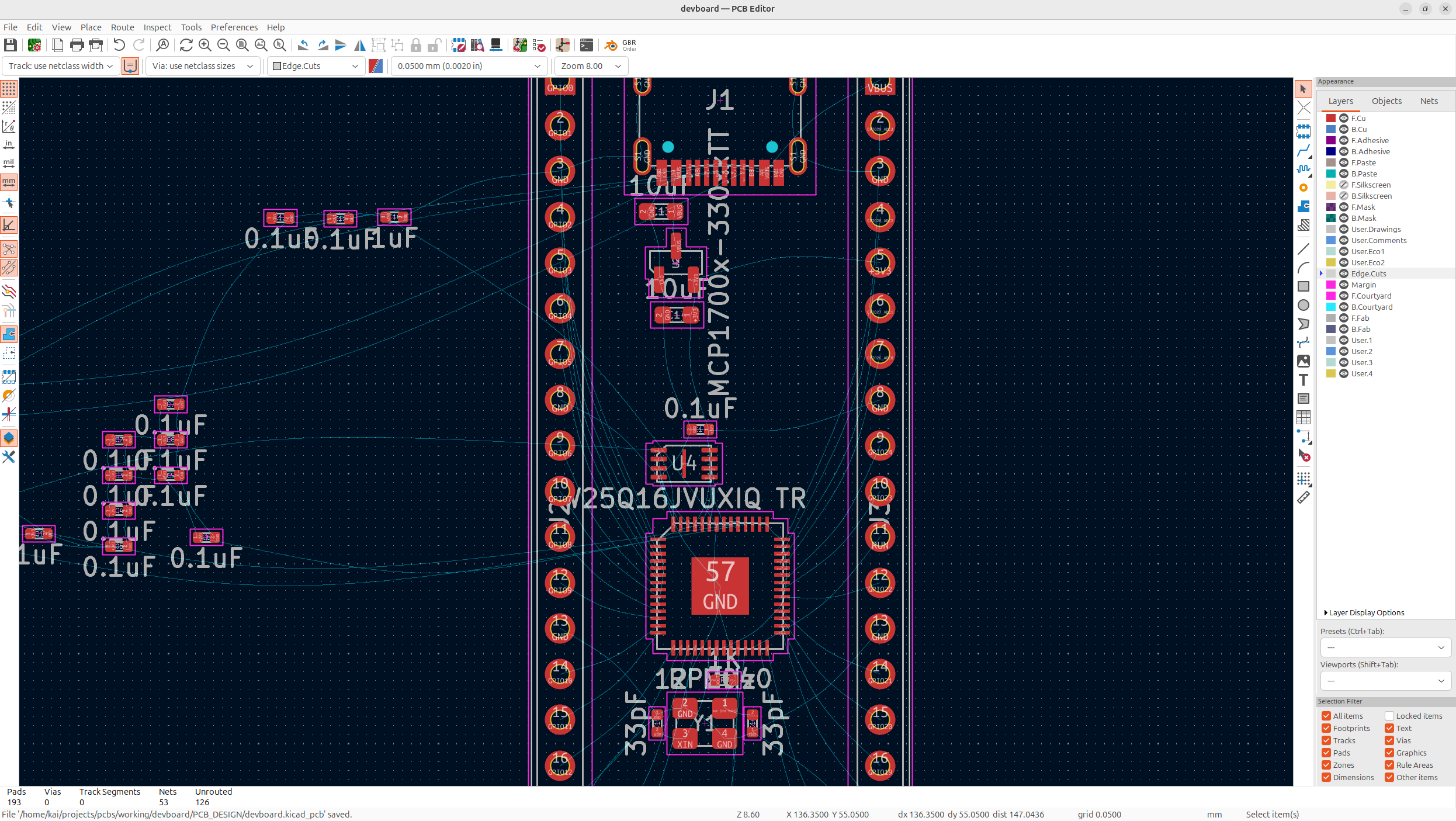
First I usually group all the caps that go together, and then I usually either start with the SoC caps, or components caps, I'm going to start with the components caps:
-
Remember, caps go close to whatever they're decoupling. Now all the RP2040 caps are grouped together, and this is because it's just a general rule to have one cap per VDD pin, and then the larger cap/bulk cap near the largest group of them:
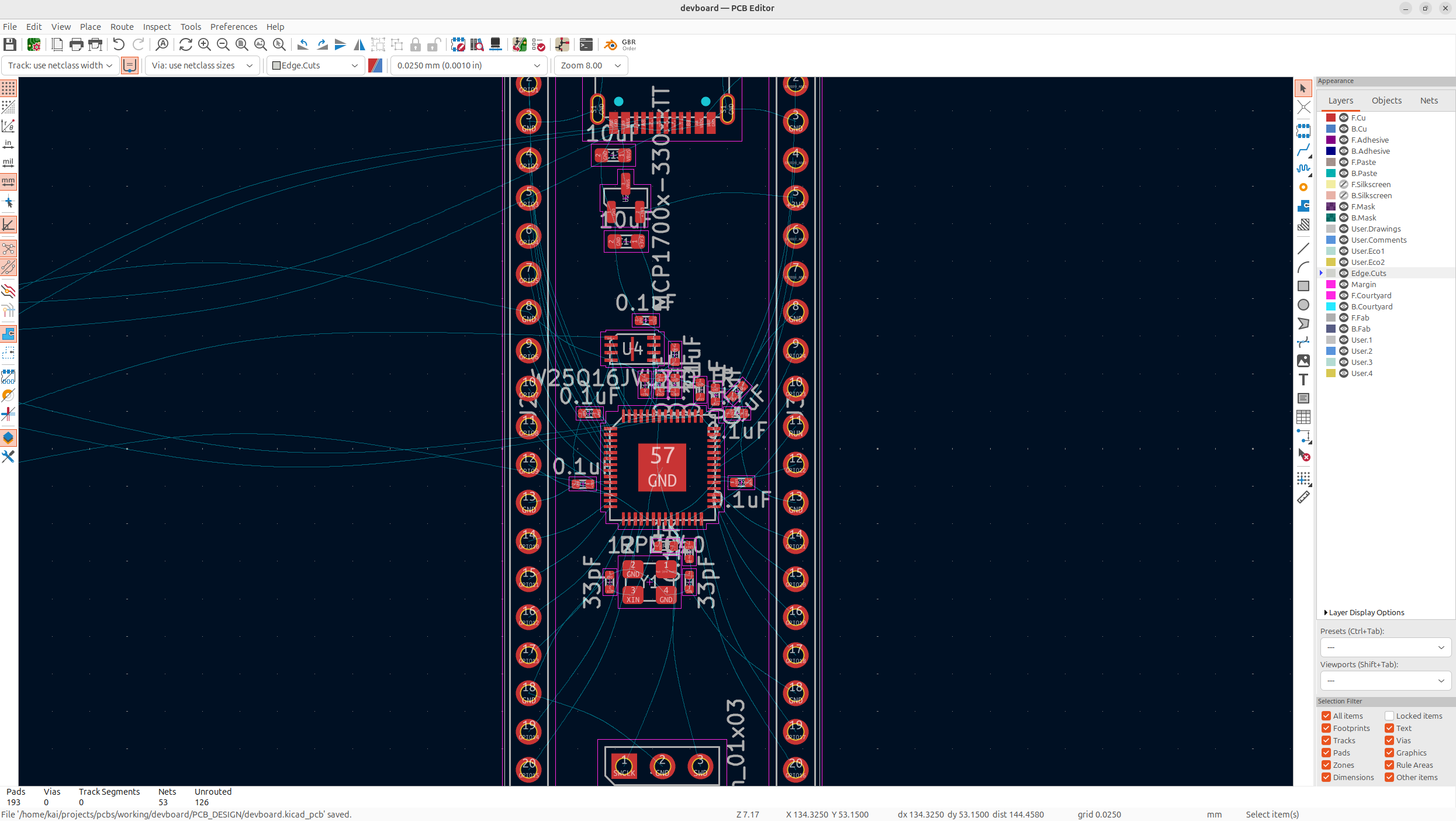
This is the layout I decided on, some of my thought process for this layout was:
- Leave enough space to route the USB differential pair
- Be able to route QSPI without via's for fast signals
- Leave enough space by the crystal to be able to route those traces
And I'll still definitely actively update it while I route my traces, but this is a good starting point.
Now all that's left to add in, is our resistors, but I'm going to actually put these to the side, and start routing a couple things! This is because it's going to be easier to place components not in the way of where traces are going to go.
#Routing
#Route the flash first
-
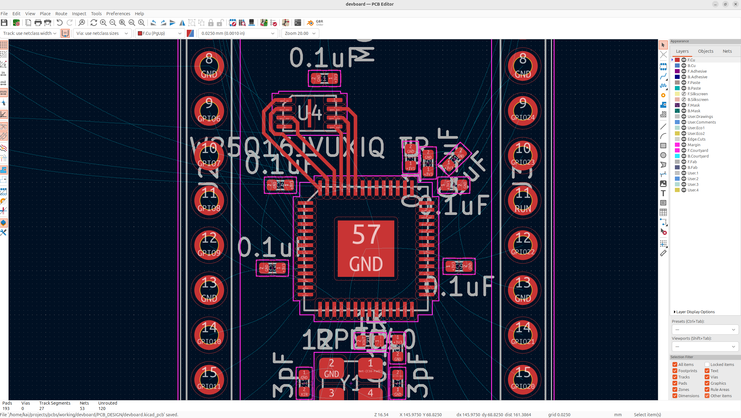
The first thing I'm going to route is my flash memory, I'm going to move the capacitors away temporarily while I do this and then add them back on later. So tap on the route single track in the right hand toolbar, and then route all the signals like so:
-
I usually start my route from the RP2040, and then put it into the component just because I find it's easier. I always start with routing my higher speed signals, and then do the lower ones.
#Place the USB termination resistors
-
Route the USB-C data lines. Now these lines are actually special on our PCB, these need to be routed as differential pairs, basically perfectly even traces, next to each other. This is because they're carrying high speed data, so the traces need to be the same length so that data arrives at the same time.
-
The termination resistors for these data lines also need to be right by the RP2040 pins to smooth the signals. I'd suggest placing these perfectly evenly apart, centered on the pins so it's easy to route our differential pairs:
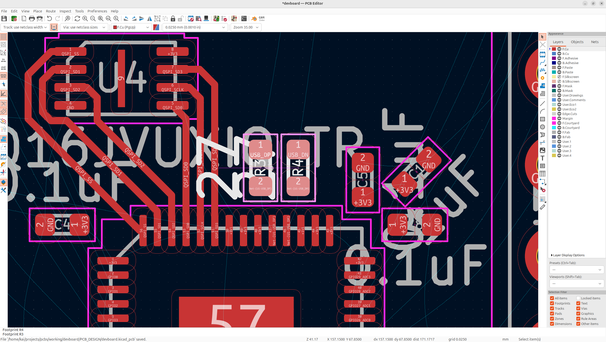
#Route the USB differential pair
-
First wire the USB D+'s/D-'s together:
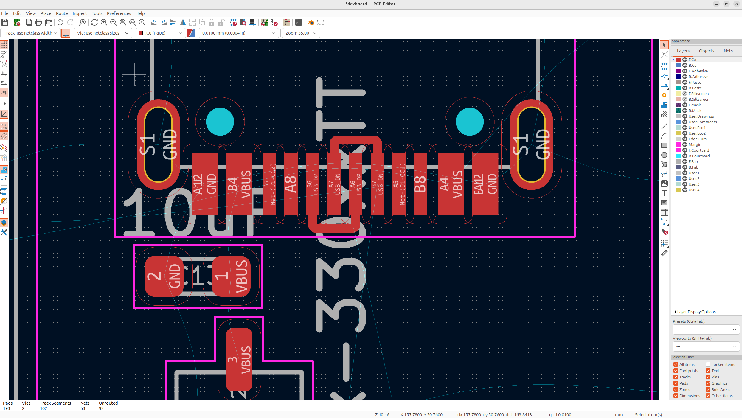
-
Then, hold the route tracks button, and go over to the symbol with 2 traces on it, or just tap 6. Then, go over to your USB-C, and tap on one of the D+/D- pins to start the trace, and route it down to your resistors.
-
If the traces won't go into your resistors pads, that means that your resistors aren't evenly positioned, you can just the relative positioning tool to do this.
-
And then you can just route the resistors nets into the RP2040 nets (Make sure they're centered so the traces are the same length, you could technically do this as a differential pair if you change your schematic slightly, but it's fine if you just position properly):
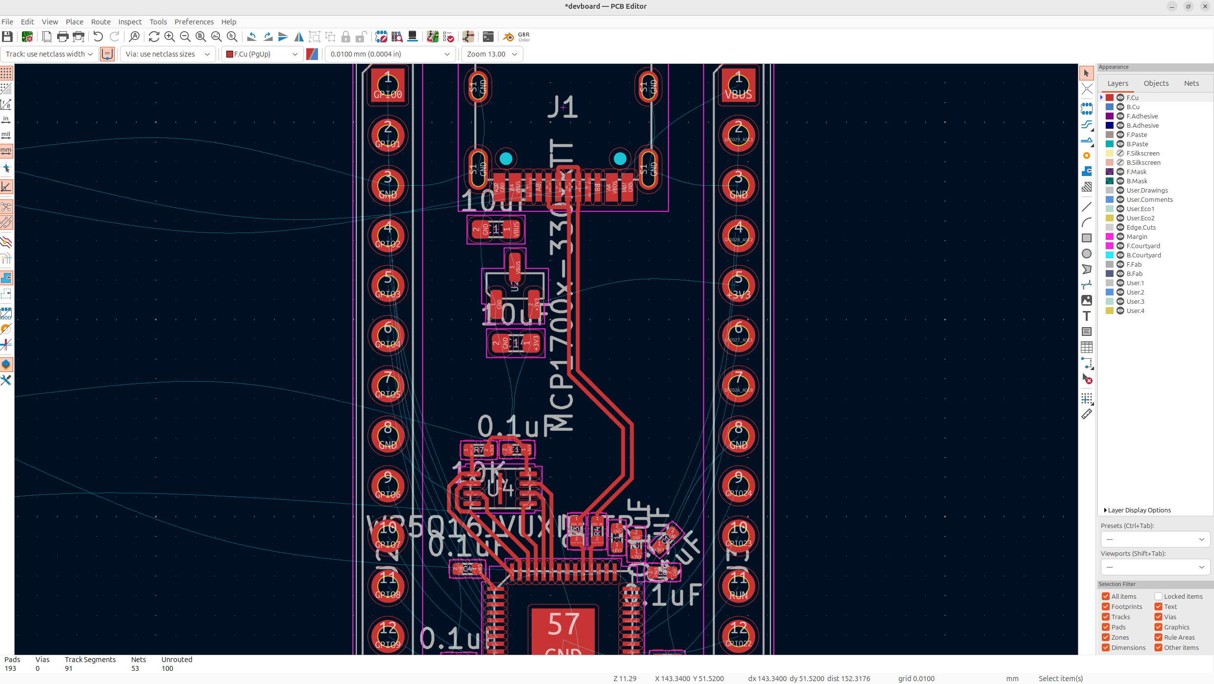
-
I added left a space inside of the USB traces for the decoupling capacitors to go.
#Match trace lengths
-
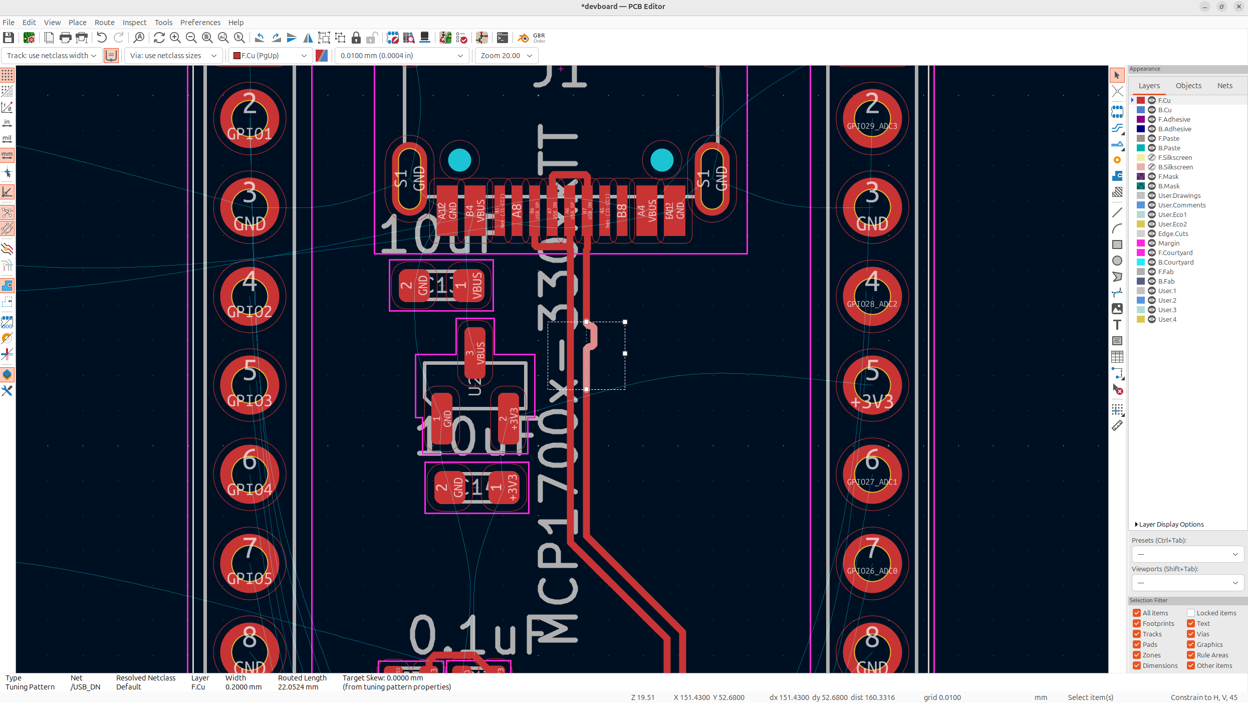
We need to make sure all these traces are the same sizes, you can check the resistor traces by using the Tune length of a single track tool on the right toolbar, they should be the same length if you did it right:
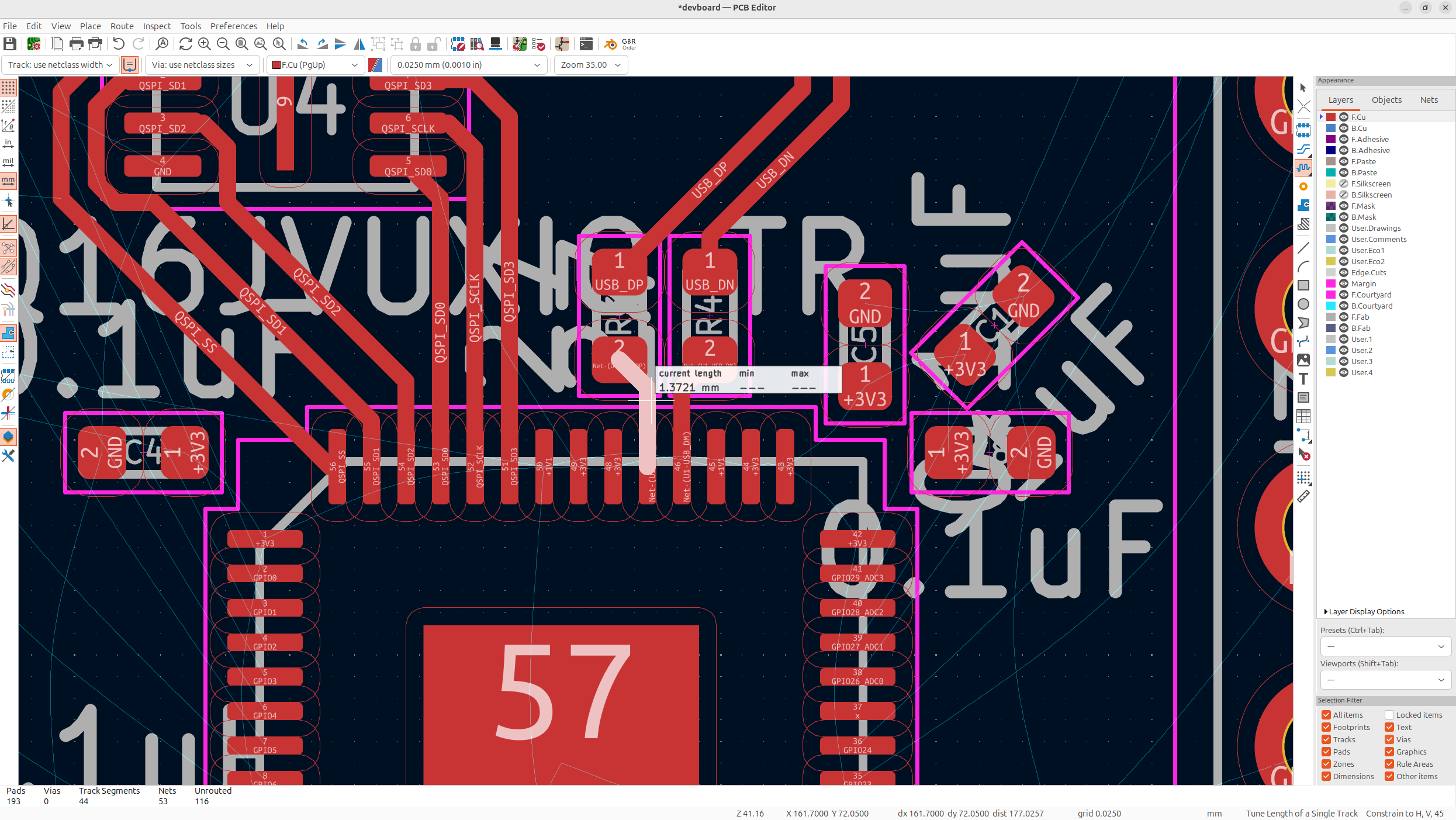
-
Your USB-C lines, are probably not the same length, so we need to fix that. You can do that by going to route → Tune skew of a differential pair in the top menu, and then selecting the trace with a negative skew, and just tapping it, and then tapping ok, and then just drag to make it slightly longer:
-
This makes all of our traces the exact same size, so that we have proper data flow!
Now we just need to wire the extra pair of D+/D-'s on the USB-C to the route that we already have. Just wire these directly.
#Bring the decoupling caps back
Now that we have our fast signals on the PCB, the other signals are fine to go through via's, so we can put in our decoupling caps now:
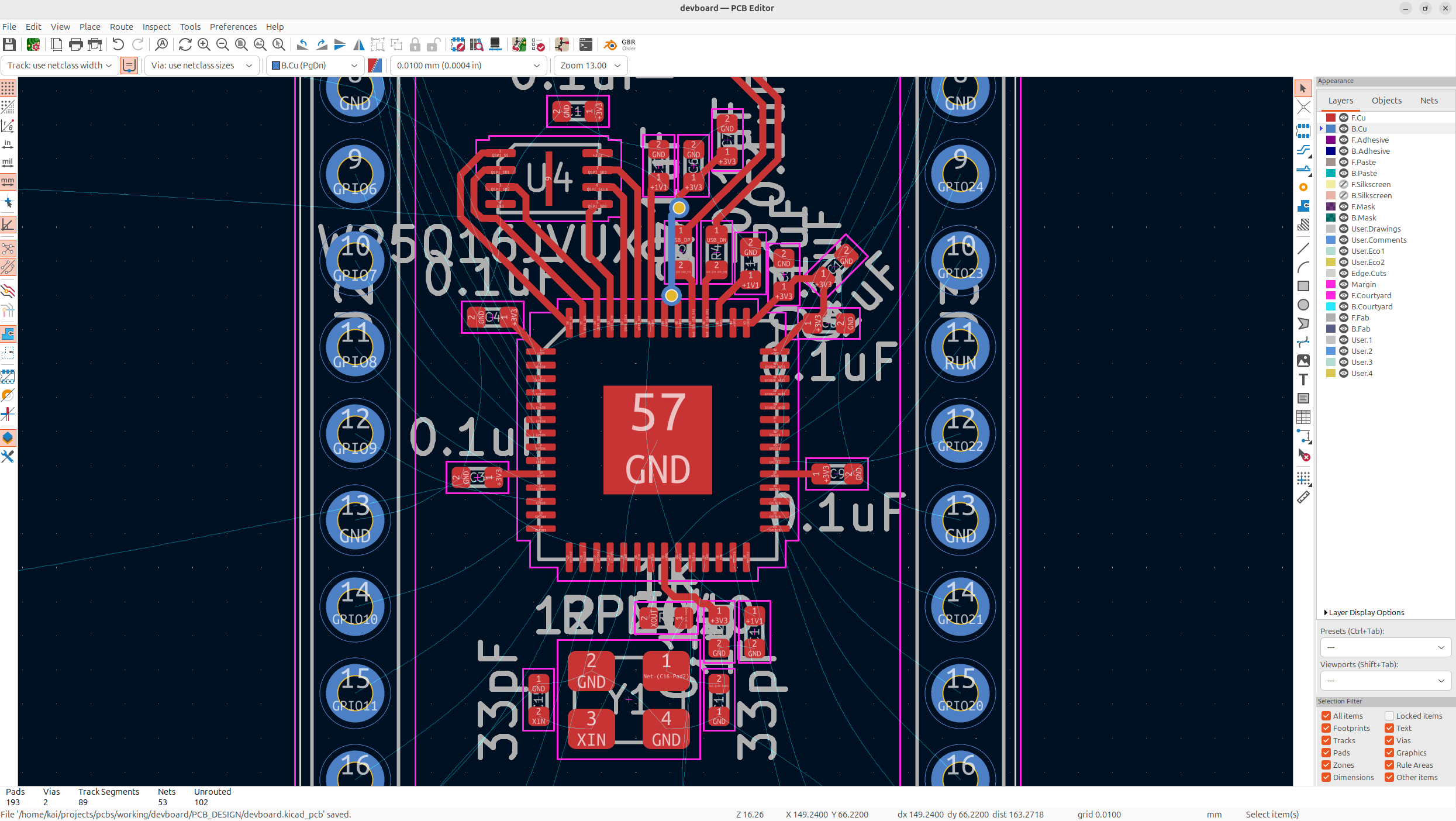
Now my routing of course isn't perfect, but I did manage to get it pretty nice and tight. You'll notice some blue on the PCB, and that's me routing on the other layer. You can change layers by tapping the other layer on the right layers view, or by tapping "v". But for SMD components, you'll need what's called a "via" in order to get to the other layer, which is essentially just a hole that allows traces to transfer to another layer of a board. Feel free to use the backside for routing if you don't have any space!
#Route the crystal, pulldowns, and pullups
-
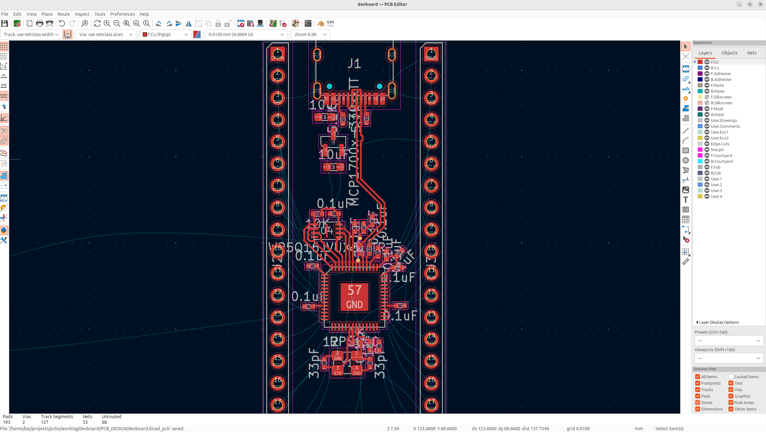
Route the crystal, the USB-C pull downs, and button pull ups, and then I'm going to leave the button/button resistor for very last because there's no specific spot that needs to be:
#Route power to the VDD cluster
-
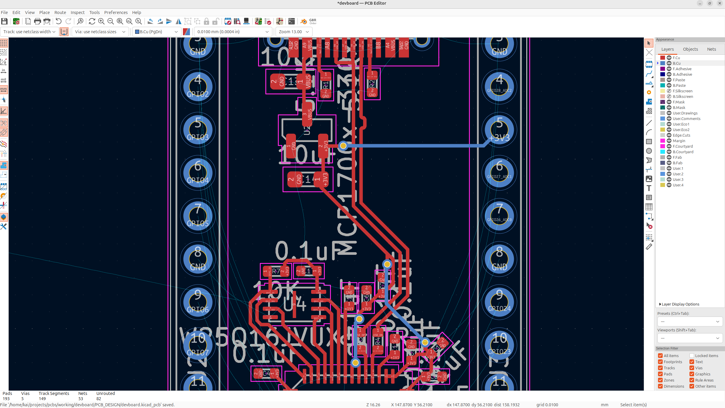
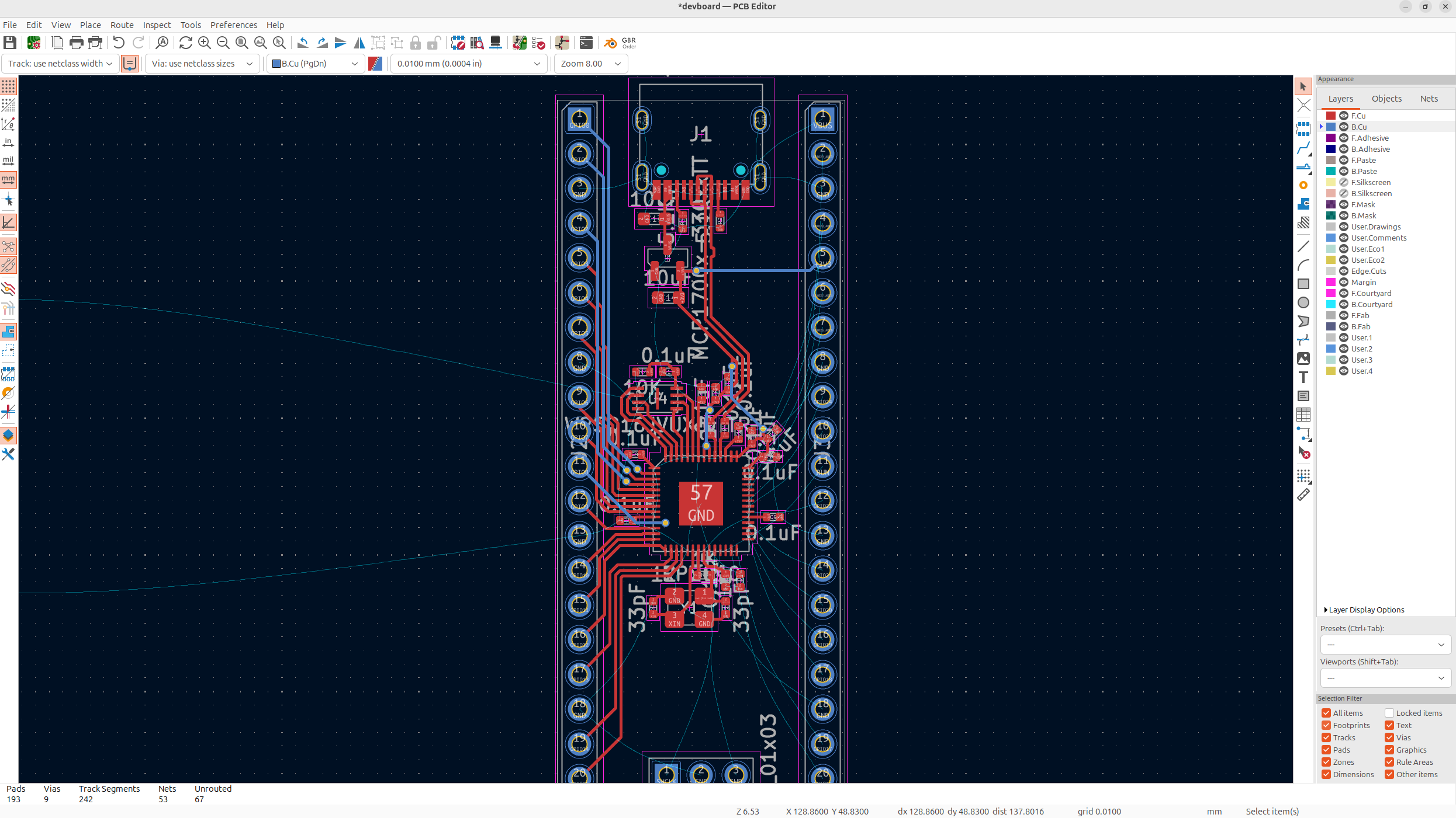
Route power to our board, I'm distributing power to the main cluster of VDD pins, and then once I'm finished routing the other signals, I'm going to route it to the other pins, just so power is even about my board:
#Route every header pin
-
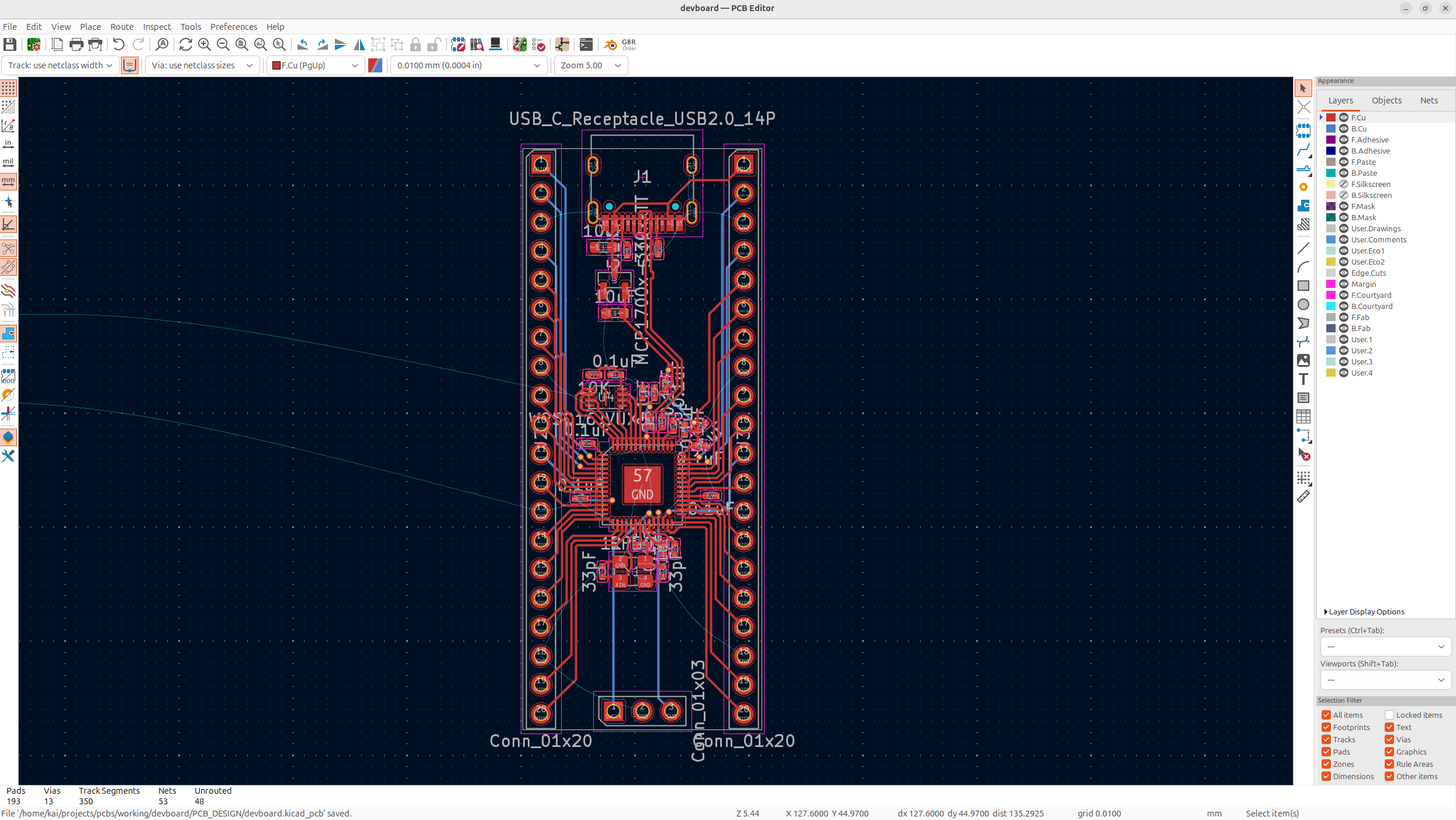
Wire every single header pin on the board, try to keep organized when doing this, and save via's/the other layer for when you have like absolutely no space left:
#Ground fill
And with a bit of finesse, all of our routing is pretty much done, we just have all of our ground signals left. Now you're probably wondering why we didn't route those. Well instead of using wires to do those, we can use what's called a ground fill.
This is basically like a giant pool of just ground on our PCB that connects all of our grounds together. We do this because it helps with signal integrity, and because there's always going to be a lot of ground signals on a PCB so it simplifies stuff. It also helps with thermal regulation!
#Draw the ground fill
-
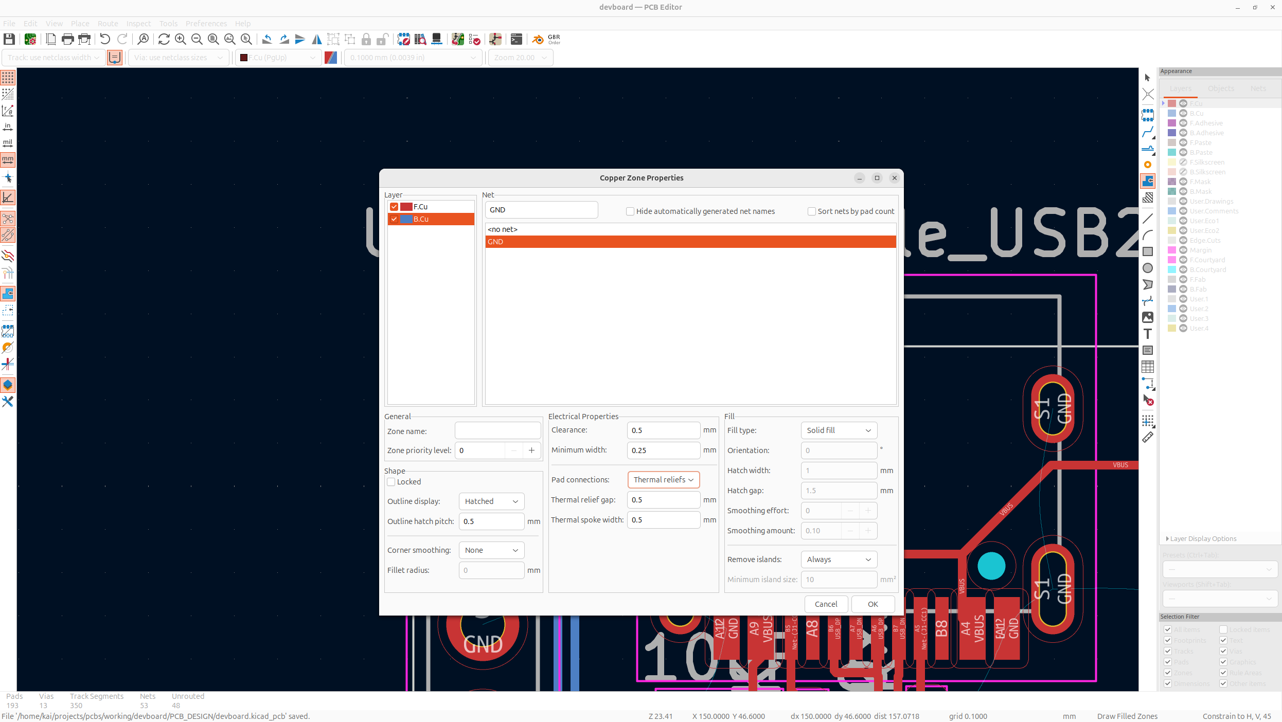
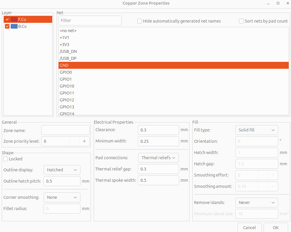
On the right toolbar, tap Draw Filled Zone, and select both layers, with GND as the net, and select Thermal reliefs as the Pad connections. Basically, with a ground fill, soldering can become harder because the fill dissipates heat, so doing thermal reliefs puts like less ground area to the hole so it's easier to solder stuff on!
-
Select the entire PCB with your ground fill, and then tap "B" to fill it:
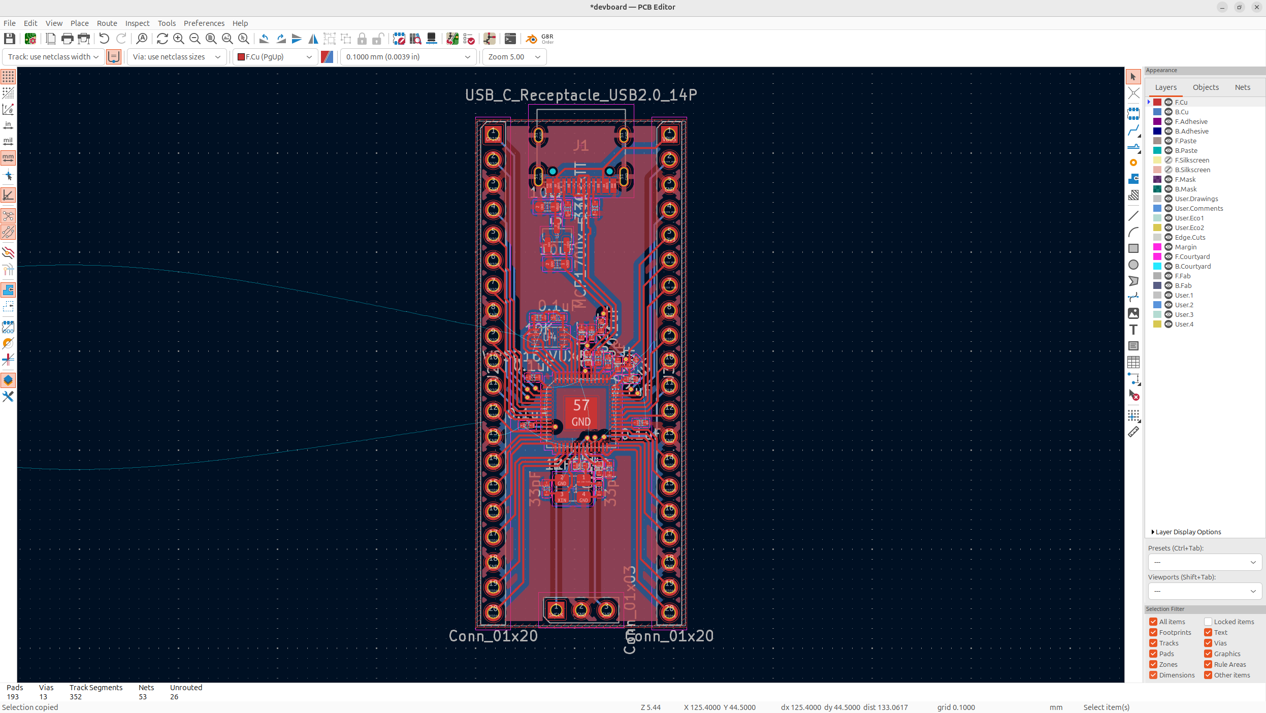
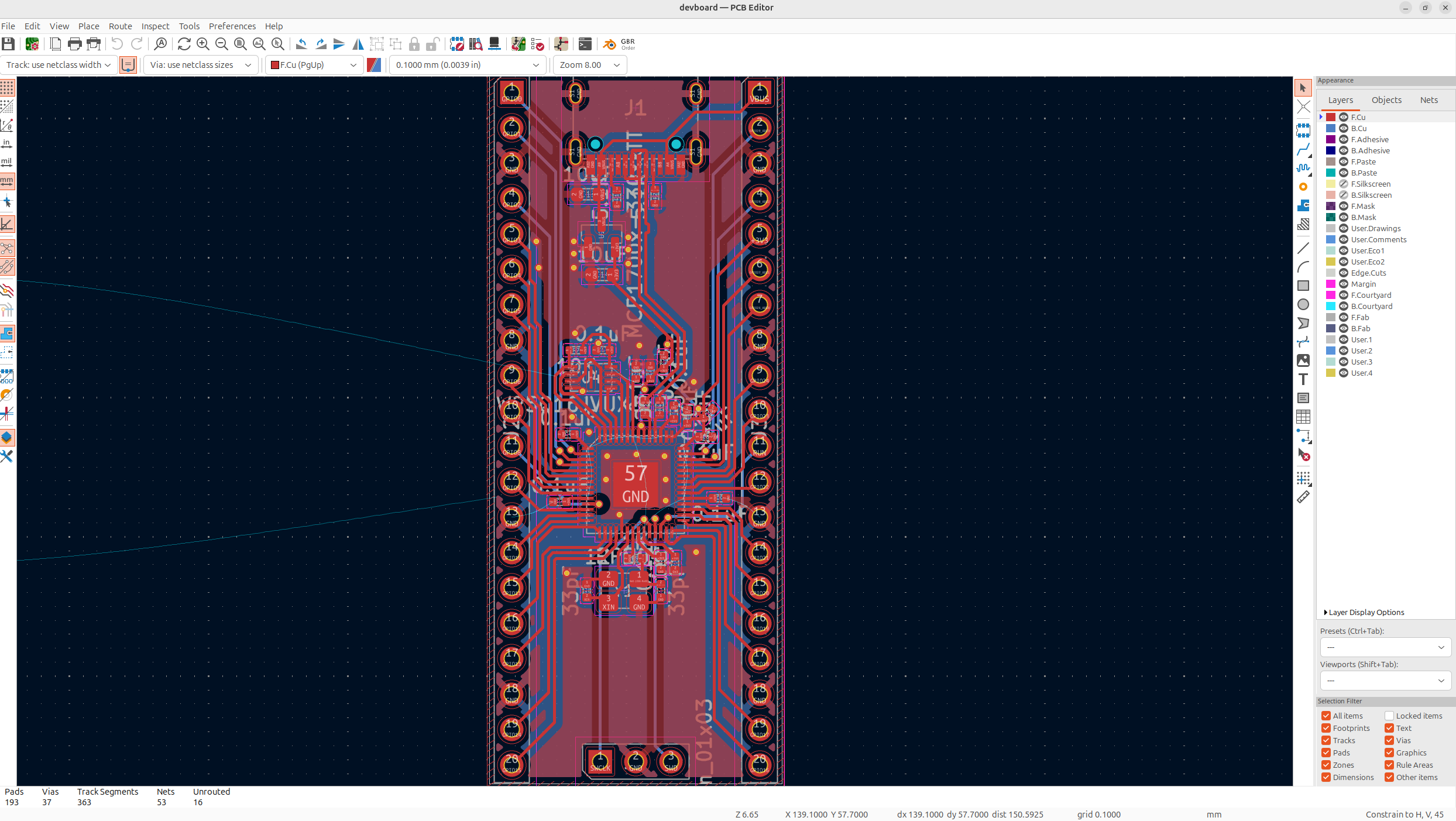
Now you'll notice that all your ground ratlines disappear. Their might be a couple that are still there though, this is because the pads are isolated, so you might need to put a via from the pad onto the ground fill. You also might need to adjust like some of the header pins signals and such to make it work!
I'd also suggest adding via's to all the isolated islands of ground for signal integrity, but this is just good practice, and also putting extra near the SoC and stuff that get's hot like the LDO:
#Place the BOOTSEL button
-
Need to add in our button that we haven't put in yet. Just find a free spot on your PCB for it, I'm going to put mine near the flash memory though because it's got some space and it's a close connection:
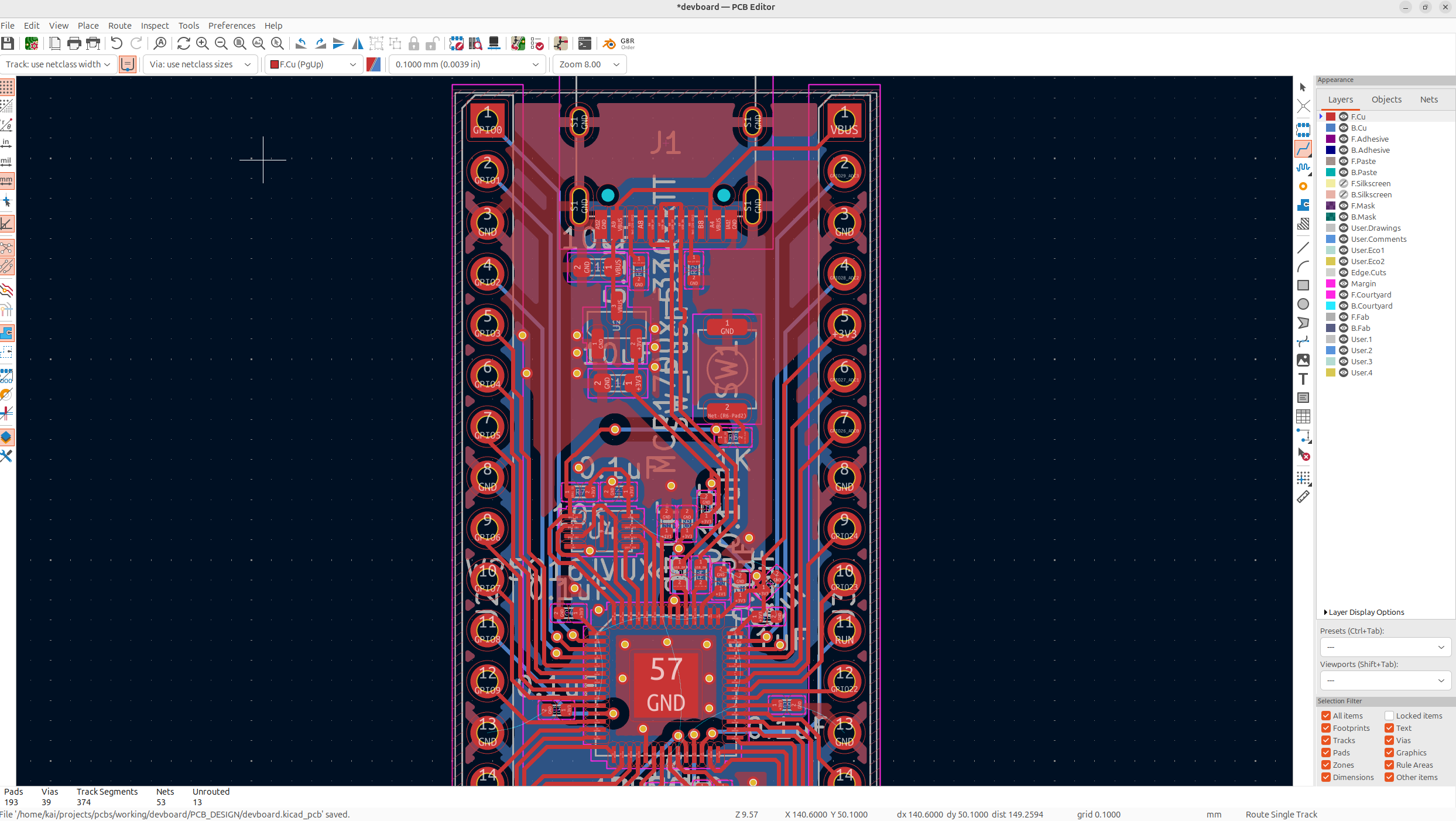
And then, if you just have any ratlines still on the PCB, just connect them up, and you'll be on the final step of designing our PCB:
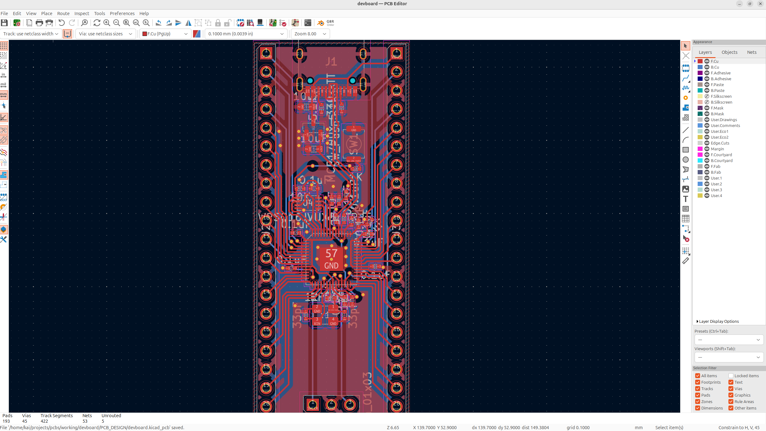
#DRC
Now you probably think, we'll we're done the PCB, what else could there be, well there's actually a couple more things we need to do. The first thing is running DRC to make sure there's no problems with our PCB.
#Run DRC
-
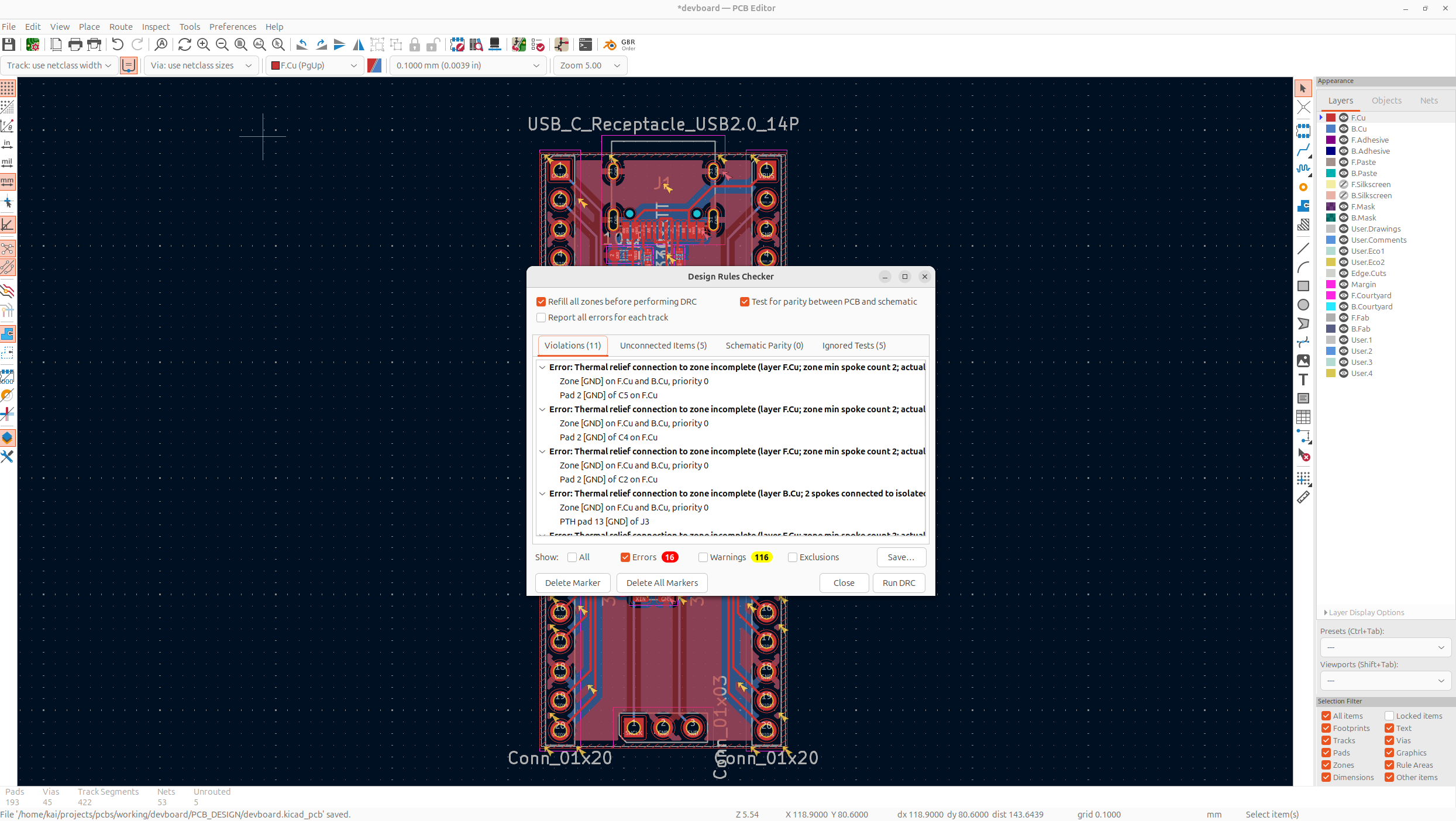
Go to the top toolbar, and run DRC:
-
My PCB has 16 errors, yours might have more, but all of these need to be properly resolved. The first things I'm going to look at is my unconnected items. These just tell me what I forgot to route, you can just tap on them to see where they are, just make sure you get all those routed before continuing.
#Loosen the thermal relief
-
Most of these are problems with the ground pour, so I'm actually going to modify the ground fill to fix a lot of these errors, I'm changing the thermal relief gap and clearance to 0.3mm instead of 0.5mm which just makes it so the traces and pads can be closer to the fill:
You'll probably also have a bunch of thermal relief errors. These require some finesse to fix, but essentially you just need to have like a thick enough ground on each component. And you can solve this by adding via's, traces, and a bunch of other stuff like editing the fill. So you'll need to research a bit and try different things to fix these. And not all of them are even too crucial, but I'd suggest fixing them all.
#Congrats on finishing your devboard 🥳
Now you've finished making your actual PCB, if you want to get an idea of how it'll look when manufactured, you can tap the 3D Viewer in the top toolbar:
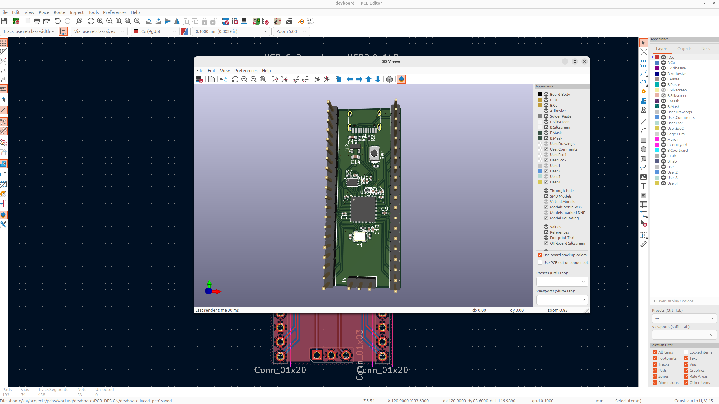
The headers will be facing the other way and you can't see the USB-C because it doesn't have a 3D model, but this is how your PCB will look. If you want the header pins to actually be right, you might be able to flip them on your PCB, or double tap the footprint and directly change it! Pretty cool huh, but you know what would make it even cooler... Art!