Now after adding all of the pins and peripherals and knowing which pins
you are going to use, we are going to finish wiring up the STM32 with
what's called a reference schematic. If you want to learn more about
this specific type of chip or any STM32 MCU in general, there is a
documentation tab
(example)
that shows you all the implementations/peripherals that you can have with
the STM32. After scrolling around, I found a
reference design
to use with our STM32.
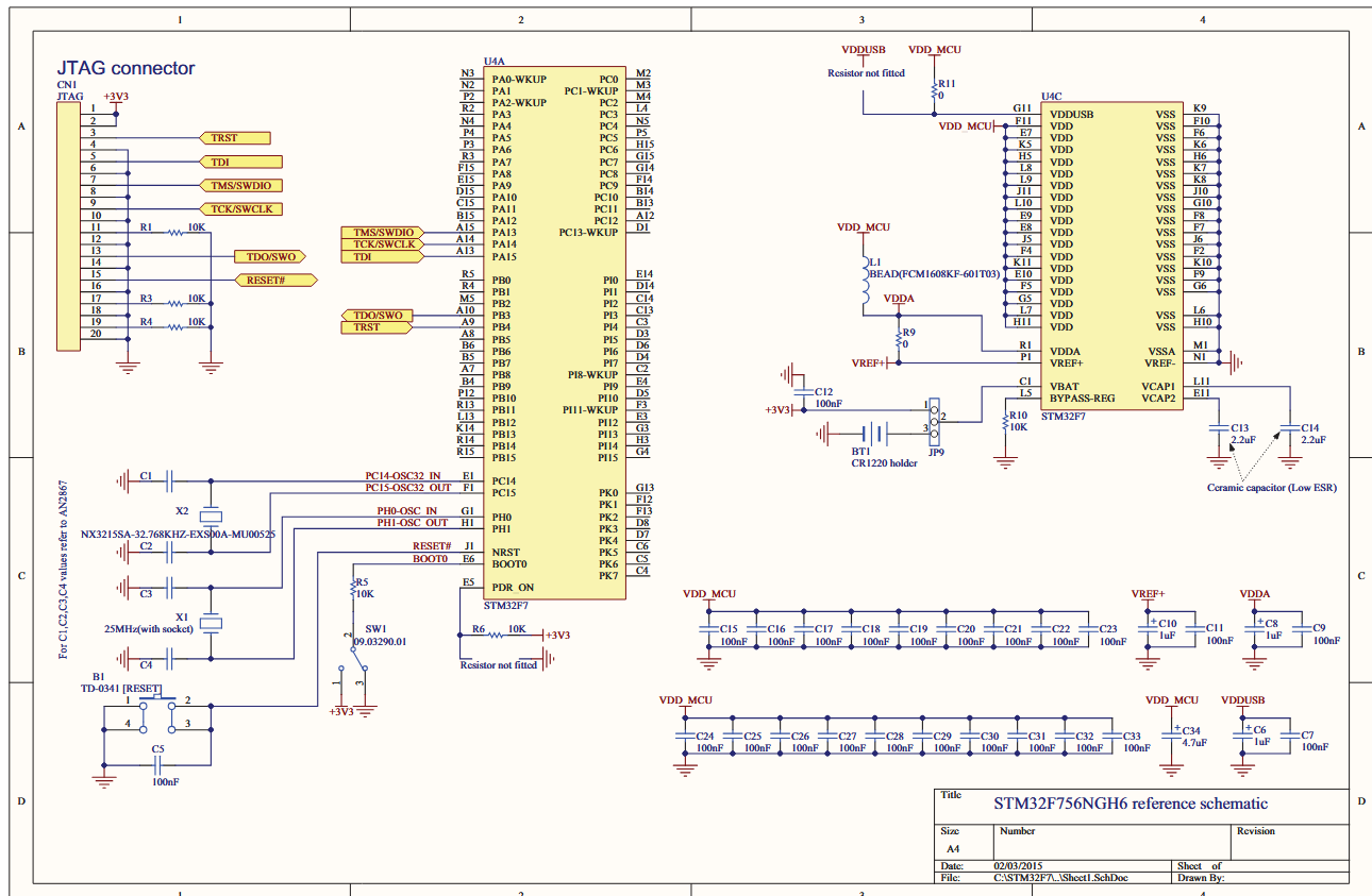
Going to the section named Reference Design, we are greeted with this:
#Wiring up power
Starting with the decoupling capacitors (capacitors that are placed near
ICs to stabilize voltage on power supply lines—they are in parallel with
voltage and connect to ground), it is generally good practice to place
one 100 nF per VDD pin and then use a bigger 1 µF capacitor per
section (e.g., VDD/VDDA/VBAT). Finally, finish off with a big 4.7 µF
or 10 µF capacitor on the main voltage line before the STM32 to
handle larger voltage spikes.
If you have analog voltage (VDDA), it's also good practice to put a
ferrite bead (like a capacitor, but it suppresses high-frequency noise
currents) before connecting it to VCC to prevent noise from digital
switching from interfering with sensitive analog functions.
It is also needed to place a 2.2 µF capacitor in series with VCAP and GND.
#Wire the STM32 VDD/VSS pins
-
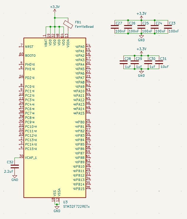
Based on this information (and the schematic), try to wire up your STM32's VDD/VSS pins (VSS is GND, by the way). You should get something like this:
-
I placed the capacitors off to the side to make it look cleaner, but it's the same as if you were to connect them directly. Just make sure that when you are placing/routing them on the PCB, they are AS CLOSE AS POSSIBLE TO THE PIN THAT THEY ARE DECOUPLING OR IT DEFEATS THE PURPOSE.
#Clocks
Looking at the reference design above, it shows that we need some buttons for the reset and boot pins. These buttons allow us to restart the MCU and allow it to boot into its bootloader to allow for programming through USB.
We also have to add the 32.768 kHz and 25 MHz clocks mentioned in the datasheet. These clocks are important for PWM and other functionality that requires timing that you may want to add.
#Import the clock parts
-
I am going to import all of these parts from LCSC using the script that we used before (including the ferrite bead). Here are the updated part numbers:
- C720477 (Button)
- C9006 (25 MHz Crystal)
- C32346 (32.768 kHz Crystal)
- C141723 (Ferrite Bead)
-
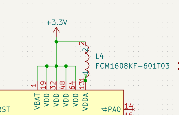
After running the script, import all of the parts in. I replaced the ferrite bead with the part from LCSC:
Now it's time to place the crystals. These crystal oscillators use a
piezoelectric (ability of certain materials to generate an electric
charge when subjected to mechanical stress, and conversely, to deform
when an electric field is applied to them) crystal to generate a stable
and accurate frequency reference signal. When using these crystals, you
need to place load capacitors:
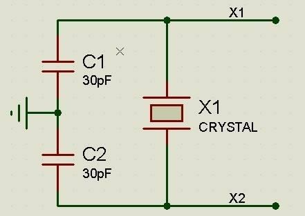
Think of the crystal like a kid on a swing. It is going back and forth at
a certain oscillation. The load capacitors would be weights that you
add onto the swing to speed it up or slow it down to get the exact
frequency. The same applies to the crystal oscillators. The capacitors
are used to fine-tune the oscillations (clock speed) of the crystal.
Each crystal has a datasheet that specifies the load capacitance that it needs, and I have already looked them up for the crystals mentioned above. REMEMBER THAT EACH CRYSTAL IS DIFFERENT EVEN IF THEY MIGHT HAVE THE SAME FREQUENCY.
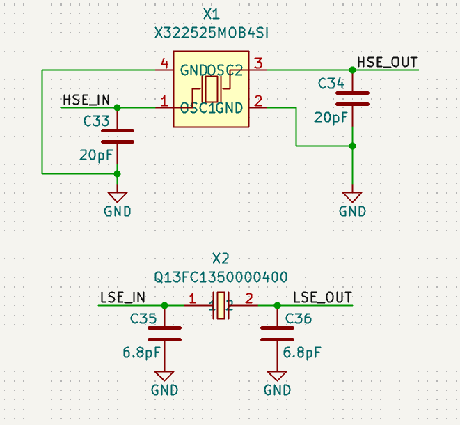
#Wire the crystals with load caps
-
The capacitors for the 25 MHz crystal should be 20 pF and for the 32 kHz should be 6.8 pF. After you're done adding them, it should look like this:
#Buttons
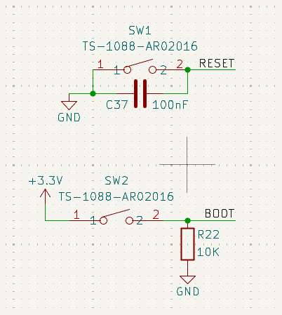
Now for the reset and boot buttons. These are super important for flashing or working with your STM32 in general. Taking a look at the reference design above, we need to connect the reset pin to a button parallel with a capacitor to ground. For the boot pin, we need to create a button that will set the boot pin to 3.3V when we press it. (Look at the datasheet to learn more.) This allows us to change the boot configuration depending on whether the boot pin is a 1 or a 0.
#Wire the reset and boot buttons
-
In the end, it should look something like this:
#Servo headers
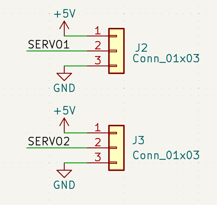
Almost done, just need to add in some 3-pin headers to control the servos. They typically have a pinout of 5V - PWM - GND so it's good to keep the pinout in that same order.
#Add the servo headers
-
Mine looks like this in the end:
#Finish the schematic
Now all that's left to do is to finish the schematic by adding net labels on all of the pins that we have used in STM32CubeMX. Your layout might look different from my layout if you're using a different chip or sensors, but here's how my STM32 looks after adding all of the net labels:
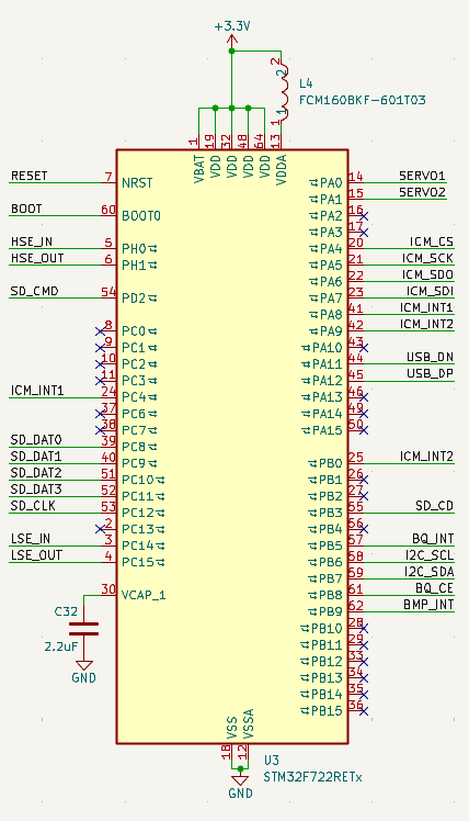
For the USB lines, DM = DN, and DP = DP.
For the ICM SPI lines, SDI = MOSI. (For the ICM, it's an input, so it would be MOSI (Master Out Slave In) for the STM32.) By that logic, SDO = MISO.
Note that for the I2C lines, I changed the names to be able to connect to each of the devices like so:
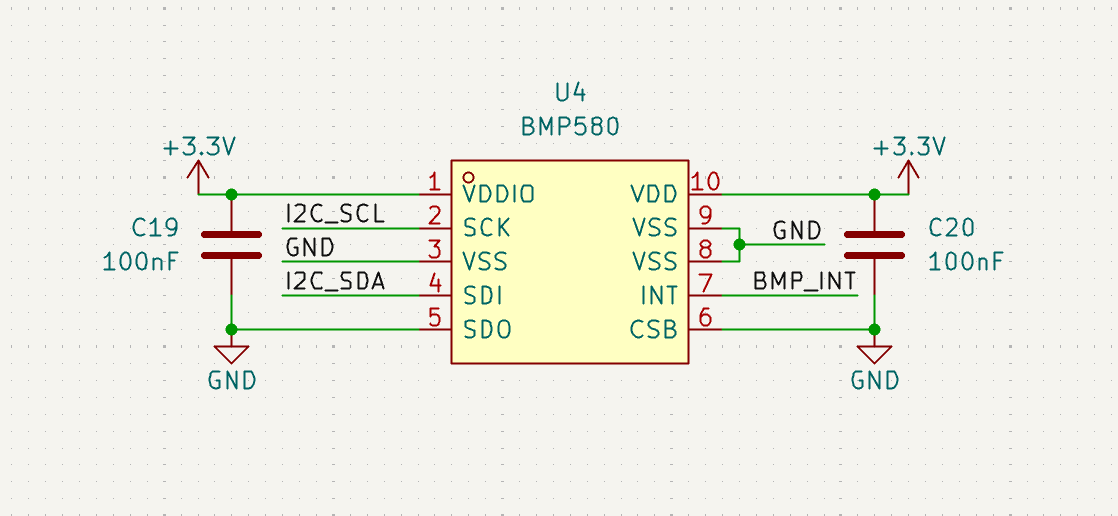
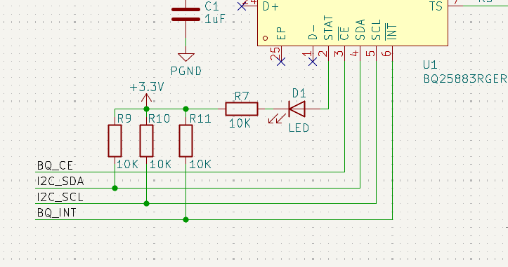
You may have a different pinout than me, but as long as you know which pins you are using and for what, then you'll be fine.
#Organize and expand the page size
-
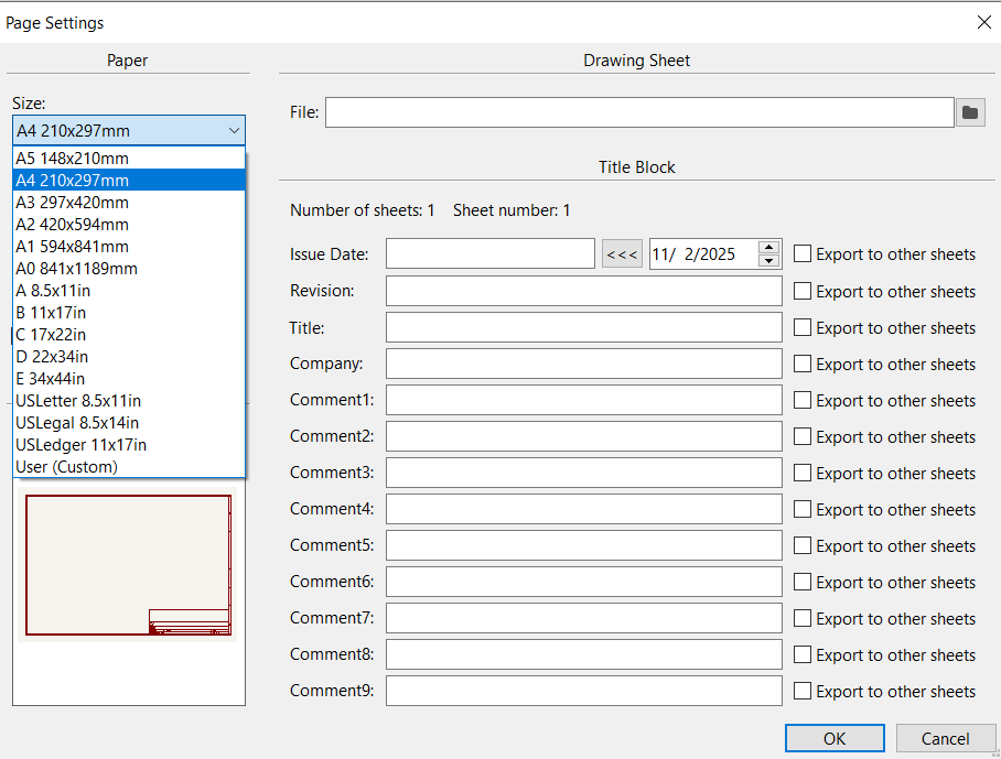
Now that you're done with your schematic, organize everything so that it looks nice. You might have to change the page settings via
File > Page Settingsin order to change the size of it: