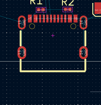
Now go to the PCB section in KiCad. There's a button at the top of the
schematic page that says Switch to PCB Editor to go there.
#Import components from the schematic
-
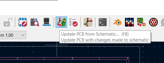
To import all of our components from the schematic, we hit this button:
-
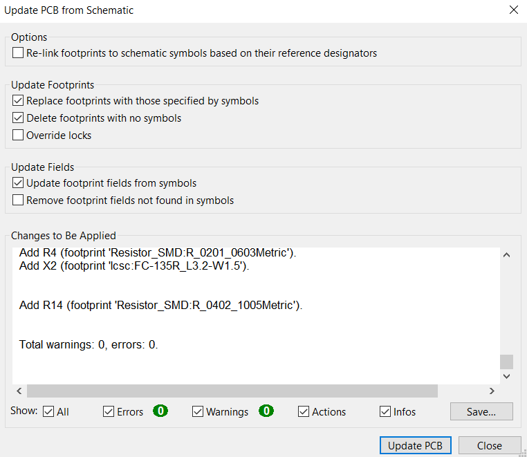
A screen should pop up:
-
There should be no errors or warnings. Then press Update PCB to import everything from the schematic.
-
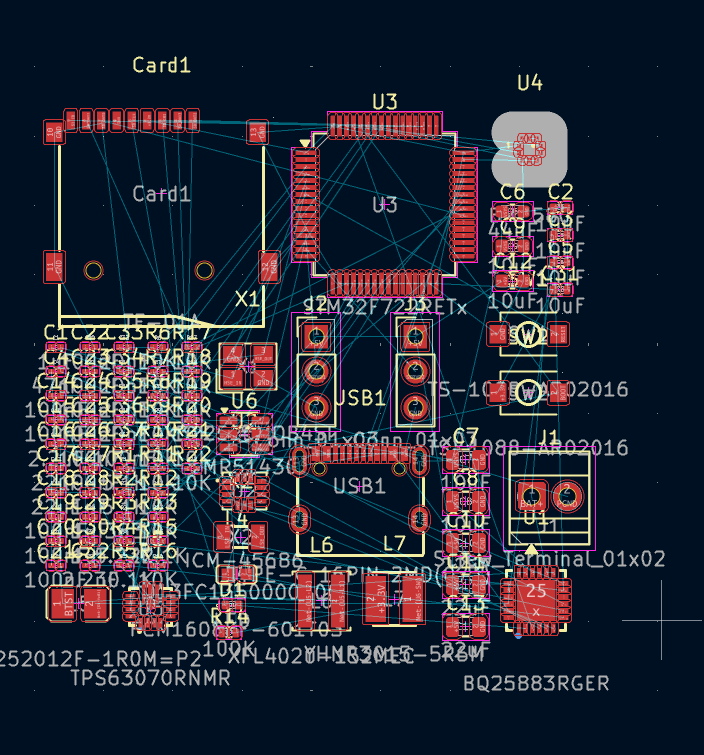
Now comes the fun part, part placement!
#But wait, what's a PCB?
A PCB (Printed Circuit Board) is a board used to mechanically support
and electrically connect electronic components. It is composed of layers
of copper and a dielectric material (a material that acts as an
"insulator" and isn't conductive). PCBs can have from 2-32 layers,
although for this board, we will be working with 2 (maybe 4 if we need
to).
In KiCad, if you look to the right, it shows the different layers:
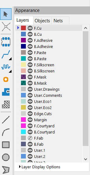
F.Cu and B.Cu (Front Copper and Back Copper) are our copper layers
(denoted by the .Cu). The only other layers that are important to us
are F/B.Silkscreen and Edge.Cuts. The silkscreen layers allow us to
put text/images and is usually that white text that you find on any PCB.
Edge.Cuts is the layer for the edges of the board (e.g., where JLCPCB
will cut to make the outline). For now we will focus on the copper
layers and routing. We can add more copper layers later in the board
settings.
Now we have to connect each of the components and route them (create
copper lines between each of them).
#Layout
I personally have always relied on this one trick to route my PCBs and it has always helped me without fail. First, separate the components into their respective groups (e.g., all of the components for the battery charger, 5V regulator, 3.3V regulator, STM, etc.), then lay them out and route them in those groups, finally put the groups together on the PCB and route the connections between them.
#Pull out the USB-C group
-
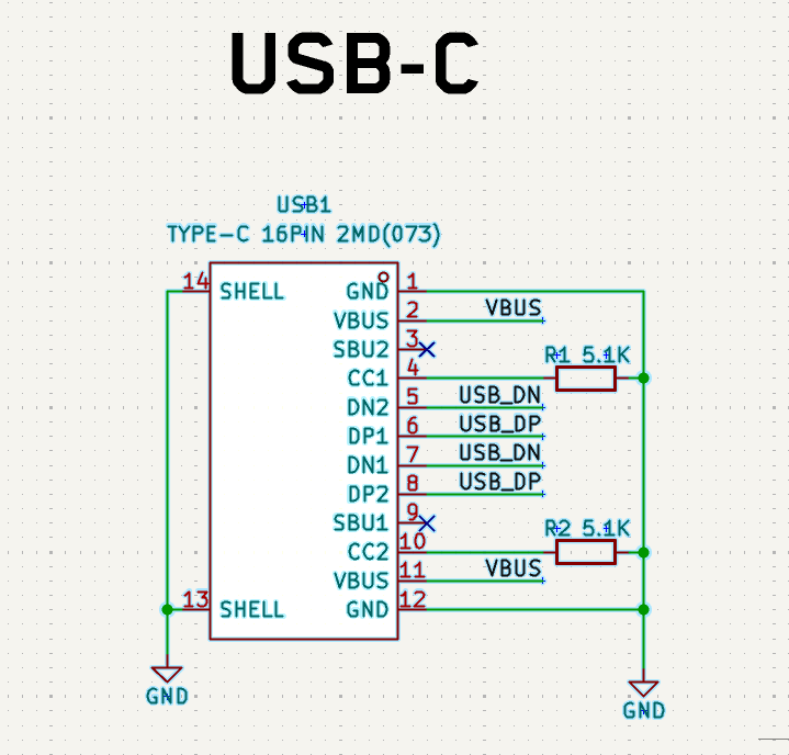
Starting with USB-C, go to the schematic and select the USB-C section:
-
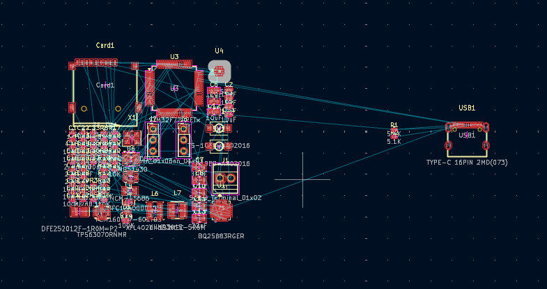
Then going back to the PCB editor, you should see that the connector and its parts are selected. Then drag them off to one side.
#Separate every group
-
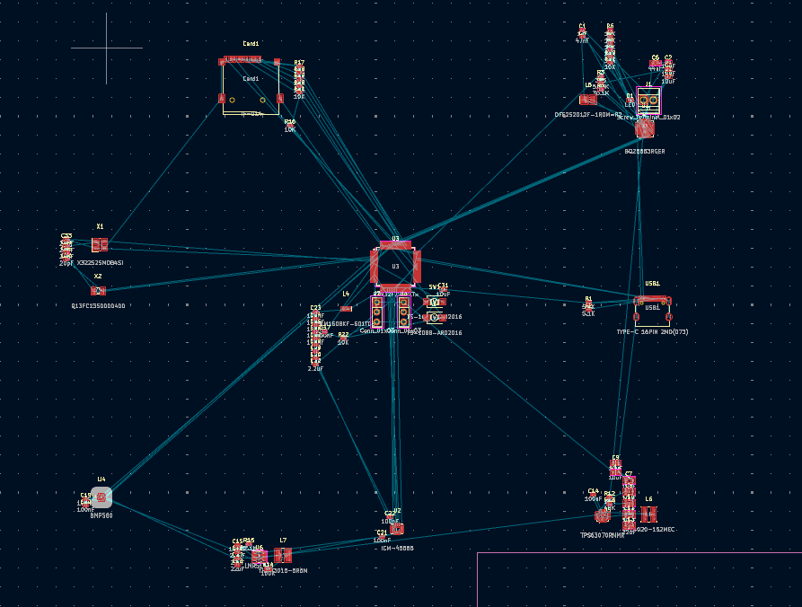
Do the same for each of the sections and after you've done that you should get something like this:
#Lay out each group
-
Now go section by section and place the components close to where they're supposed to be connected. Make sure to place decoupling capacitors close to the pins that they need to decouple or they won't work.
-
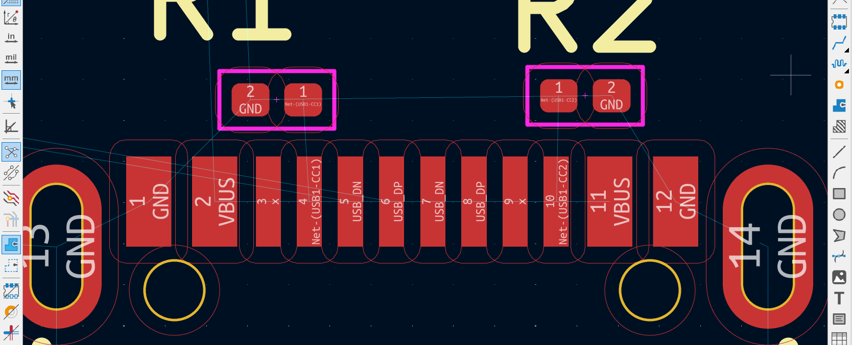
Example of the USB-C connector:
-
I placed the resistors close to the pins that they need to decouple and in a good orientation so that I can connect that ground pin easily.
-
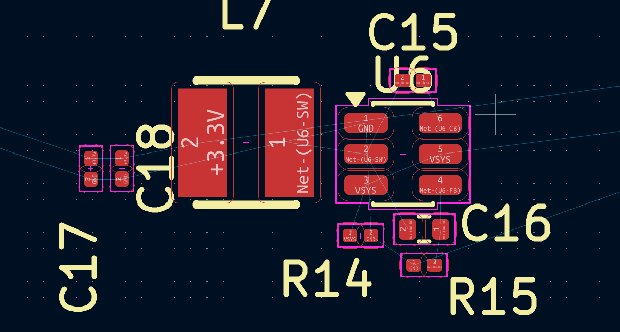
For the 3.3V Buck converter I routed it like this:
-
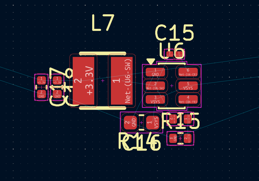
But now I'm realizing that the components I chose are too small so I am going to make the capacitors and resistors a bit bigger:
-
Ignore the silkscreen for now (the yellow) we are going to come back to that later.
-
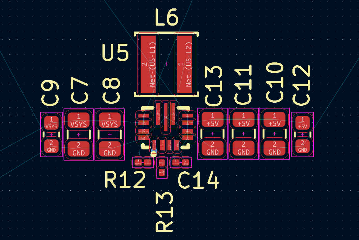
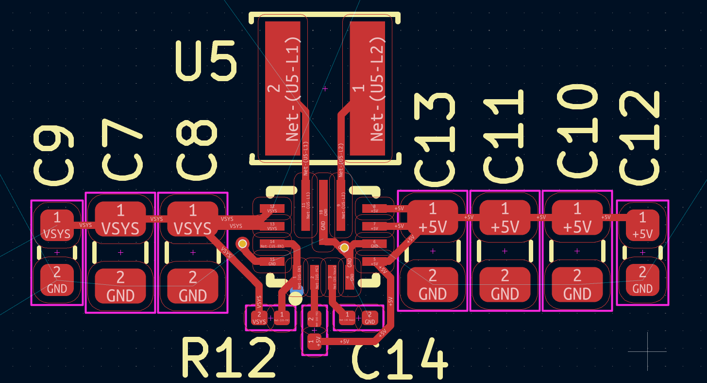
Continue on for each of the chips. For example, here is how I placed the 5V buck-boost converter:
-
As you can see, the capacitors are close to the pin and to each other, and all of the components I have placed in a way where I can create easy connections like so:
-
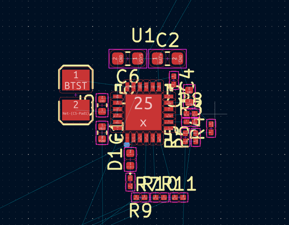
Moving on to the battery charger:
-
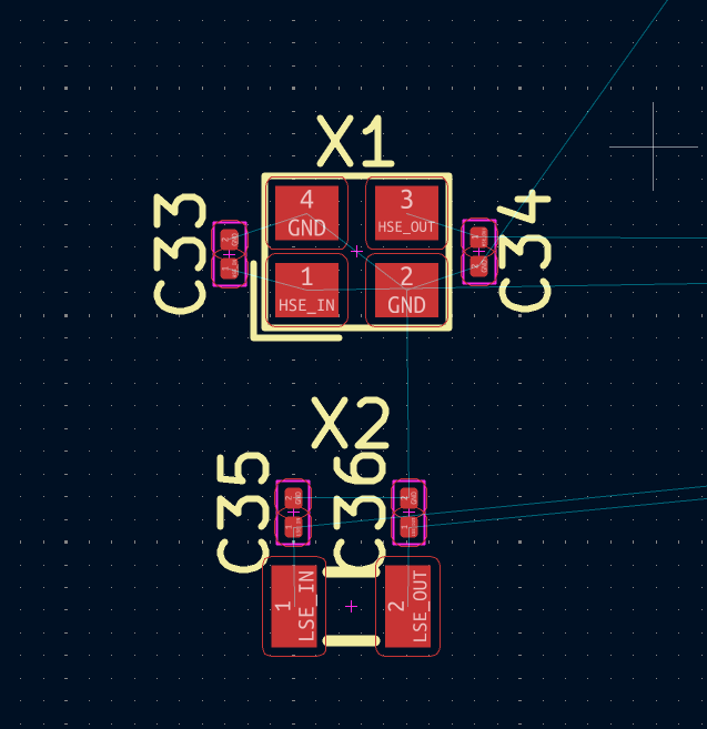
Crystals:
-
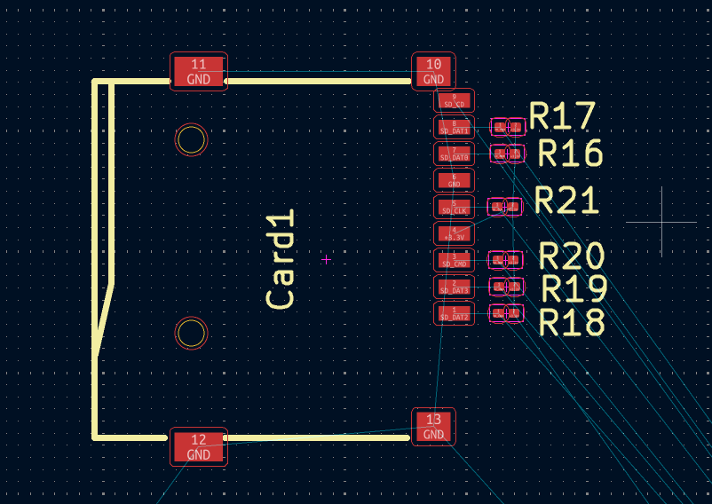
microSD Card:
#Rotate the STM32 for easier routing
-
For the STM32/microcontroller, it's a personal preference of mine to rotate it 45 degrees so that it's "easier" (subjectively) to route later. You can change this by editing the
orientationproperty: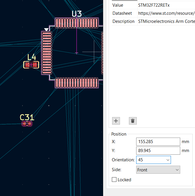
-
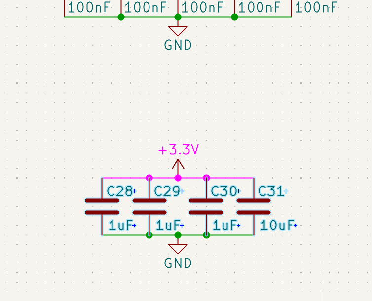
Also for these decoupling caps:
-
I changed the sizes to be 0402 as they are bulk decoupling capacitors and should always be a bit bigger than the normal ones.
-
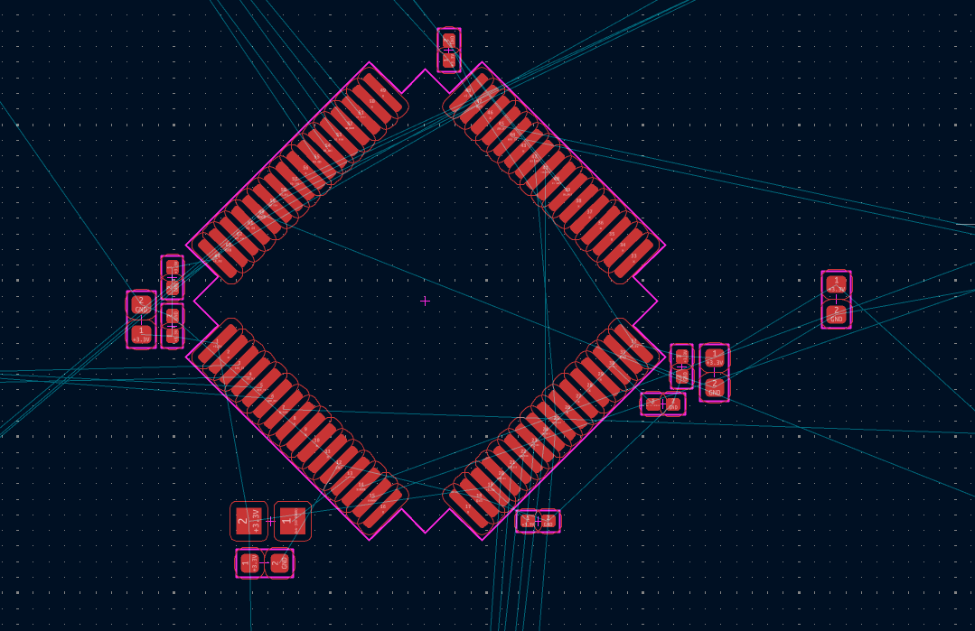
After laying out the decoupling capacitors for the STM32, it looks like this:
-
That one capacitor that is by itself on the right is the big 10 µF capacitor that I plan on laying out later depending on where the 3.3V is coming from.
#Final layout
After you're done laying out all of the passive components (resistors,
inductors, capacitors, etc.) and their respective ICs, it's time to
layout each of those groups on the board.
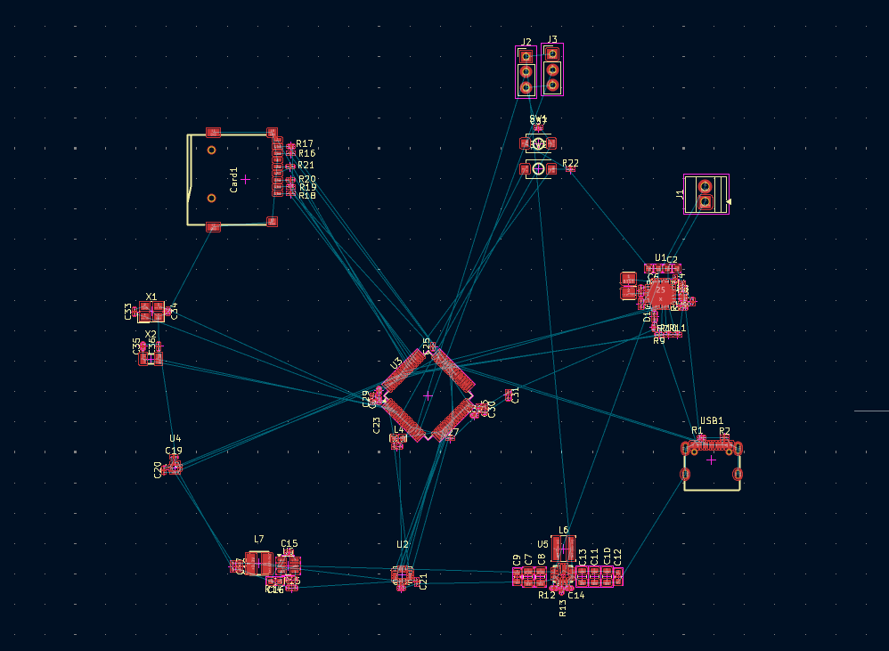
Here's what my "board" layout is and I'm going to play around with the placement of each of the groups before routing to make it more compact.
#Arrange the final layout
-
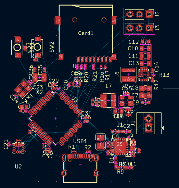
After a bit of laying out and thinking I came up with this:
-
The battery charger is close to VBUS and then VSYS has an easy path through to the 3.3V buck converter and 5V buck-boost. The battery connector is also on that side. On the top is the microSD card with a connection to the STM32 directly under it. On the top left are the buttons for boot and reset and also the 2 clocks. On the bottom left is the IMU that is kept separated from the rest to reduce noise (happened by accident lol) and the STM32 in the middle whose USB DP and DN pins are inline with the USB-C port.
-
You don't have to use this exact layout but try to have one that's "organized".
#Draw the board outline
-
Now after defining the layout, go to the
Edge.Cutslayer and create a rectangle with the tool on the side: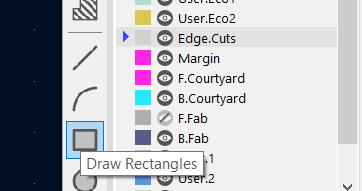
-
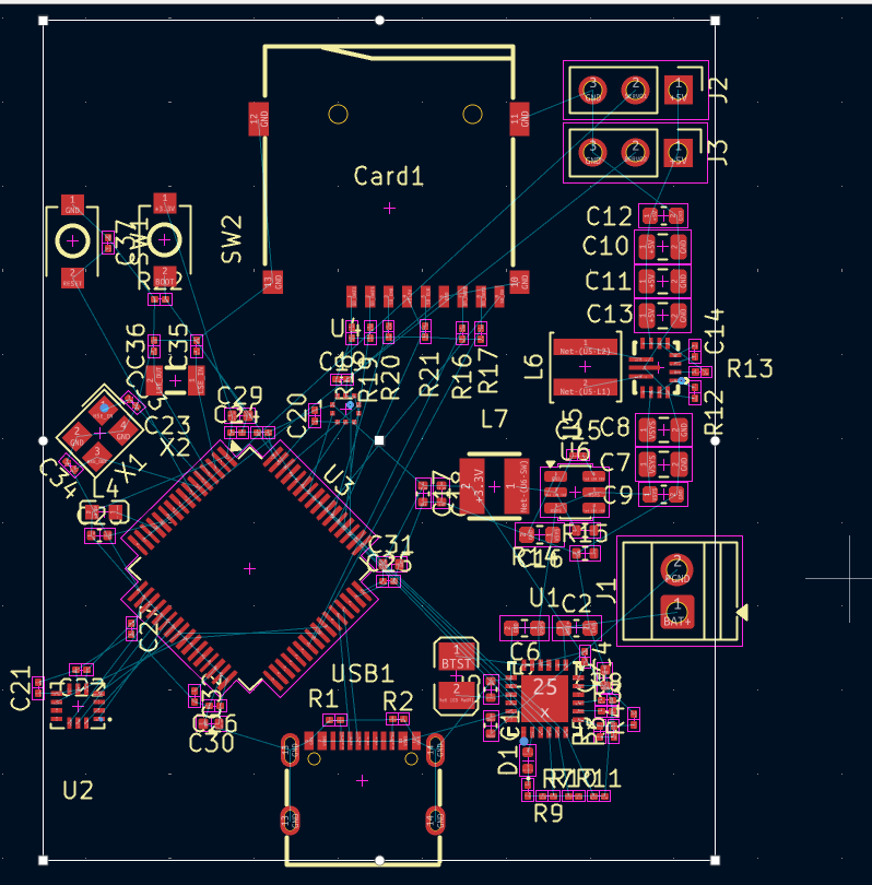
This will be the PCB outline.

-
When I originally created the board size to cover all of the parts, it had a size of 42.7mm x 47.8 mm so I decided to round it to 40mm x 46mm (optional).
-
After creating the board outline, you may need to shuffle some stuff around for it to fit. It's good practice to put the USB-C connector hanging out a bit so that you have space to plug in the cable like so: