
Now let's start wiring up the power components and USB-C. It's always good practice to start wiring the components that would be used first. In this case, it would be USB-C as it is going to receive voltage, then the battery connector as that voltage from USB-C is going to directly charge the battery. If there is no USB-C, then the battery will provide voltage, followed by the 2 regulators. Again, you can wire each component up in whatever order. I just do it like this to be a bit more organized.
#USB-C
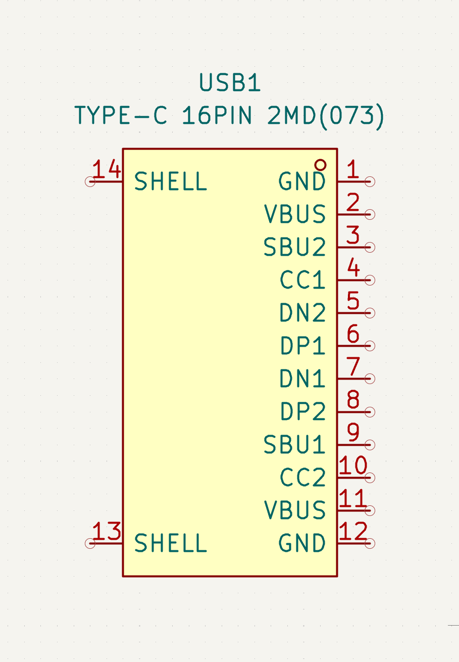
This is the USB-C connector. As you can see, it has a lot of pins, but don't worry if you don't know what all of those mean. Here's a quick explanation:
- Shell: This is the outer case of the USB-C port. It's usually connected to ground.
- GND: Ground.
- VBUS: This is the pin that supplies voltage from the device that connects to it. Usually it provides 5V at 3A, depending on the cable.
- SBU1/2: These are low-speed lines that can be used as alternate pins for different accessories, such as AUX+ and AUX- when connected to a DisplayPort. We don't need to use them.
- CC1/2: These are Configuration Channel pins. Basically, they detect if the connector is flipped and can also be used to negotiate more power out of VBUS (USB-PD). We are going to connect them to 5.1K resistors to ground as this tells the other device that we want 5V.
- DN/DP: These are the USB lines that we will be connecting to the STM32. They are used to transfer data between devices.
The CC pulldowns are the same idea as any other pull resistor, just pulling down to GND to negotiate a 5V rail.
#Wire the USB-C receptacle
-
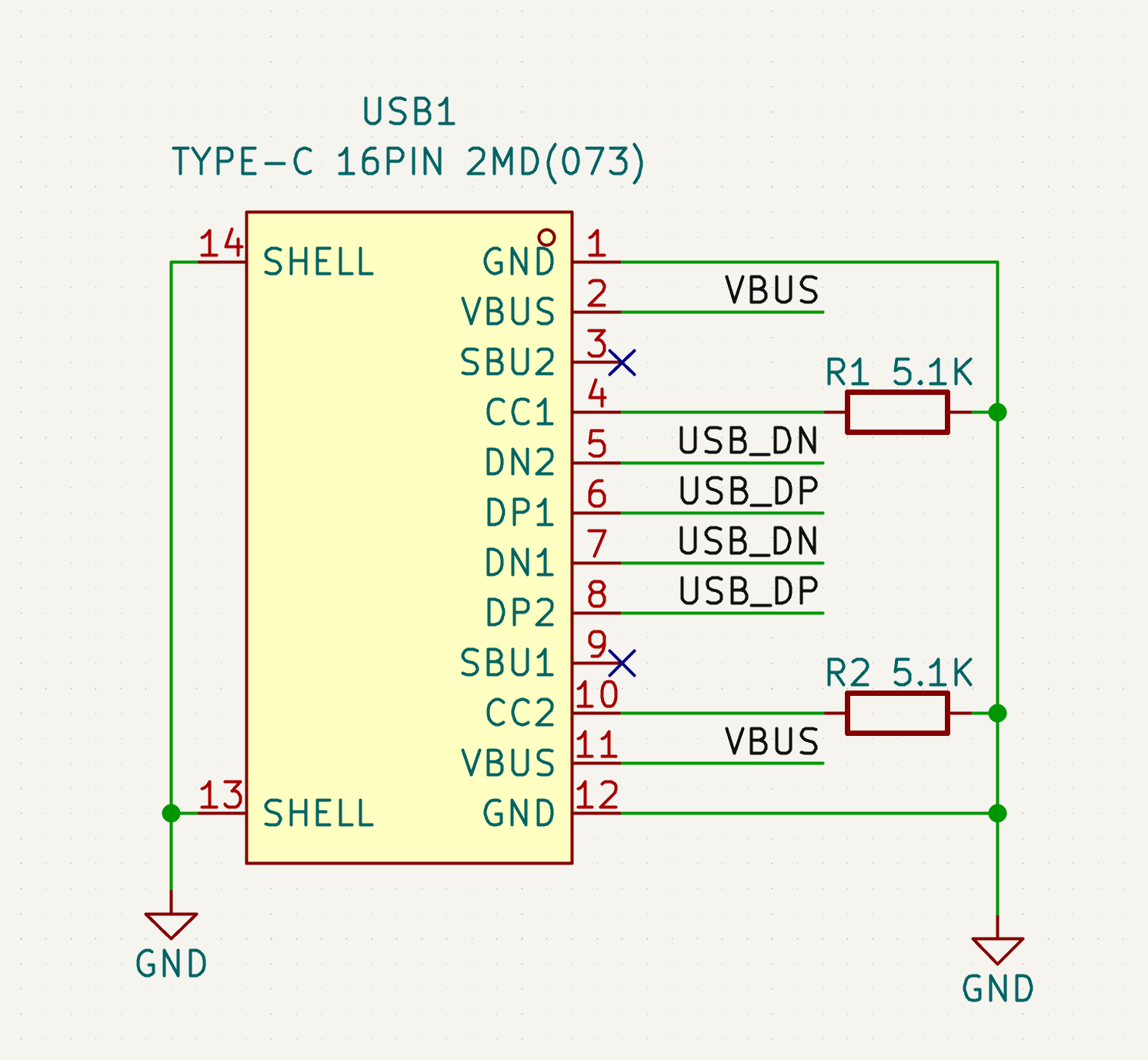
Now with that information in mind, when you finish wiring up the USB-C connector, it should look like this:
-
I used net labels to organize it better so that we don't have spaghetti cables all over the schematic.
#Battery charger (BQ25883)
Now let's wire up the battery charger. This is the next step in our power
route. There are many chips in the world, and knowing the pins on each of
them is virtually impossible. So, each manufacturer provides what's
called a datasheet for each component. It's basically a document that
details everything about that chip—its pinout and how to implement it.
To access the datasheet for any component in KiCad, simply click on the
component and press D. If there isn't one, just search on Google
"[part] datasheet" and it's usually a PDF.
Opening the datasheet for the battery charger, we are greeted with this:
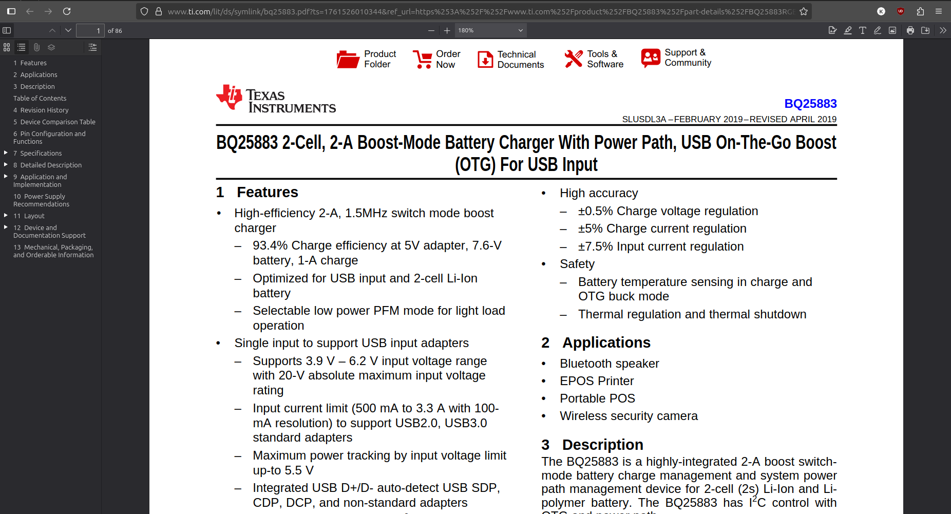
This may look intimidating as there are 86 pages of letters, numbers,
formulas, and graphs. However, there is one section that is valuable to
us called Application and Implementation. This section basically gives
us a reference schematic on how to use said chip. We can use the sidebar
or table of contents to locate that section. You should see this:
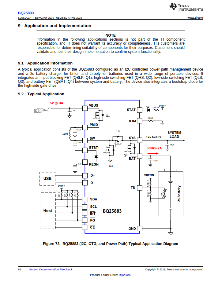
This is the schematic for a specific implementation, and we can see below that there is a table that describes it:
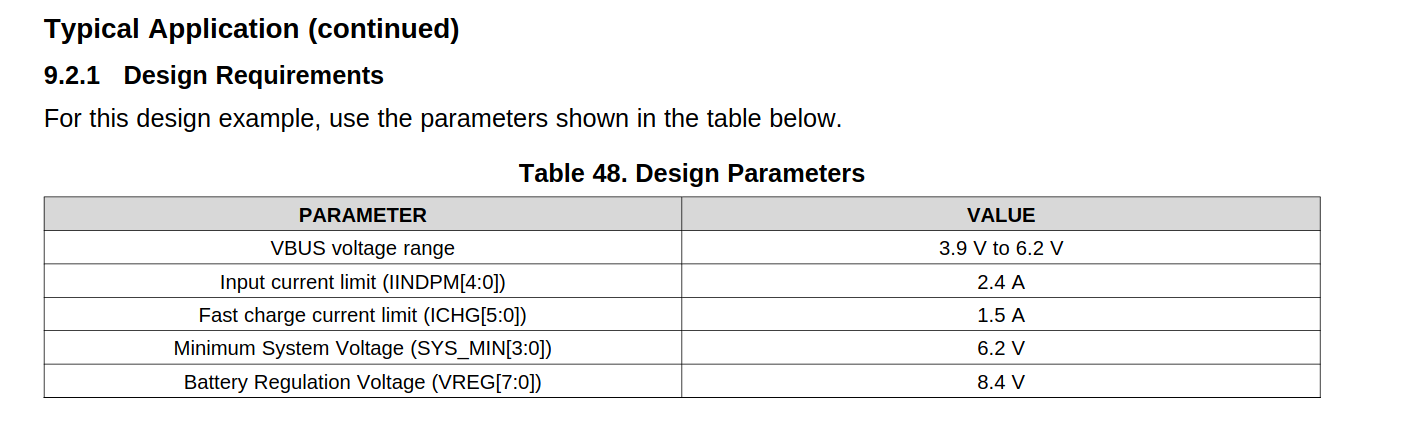
Here we can see the different parameters that influence the design of the schematic above. It is important to understand what each of these values means to determine if the schematic works for your specific needs.
#Design parameters explained
- VBUS voltage: How much voltage the chip needs to charge the battery. Our 5V from the USB-C fits within the range, so we're good.
- Input current limit: Determines how much of the available 3A current will be consumed.
- Fast charge current limit: Sets how much current will be used to charge the battery.
- Minimum system voltage: If the battery falls below this voltage, the internal regulator activates to maintain this voltage until the battery completely dies.
- Battery regulation voltage: The maximum voltage the chip will charge the batteries to. In this case: 4.2V per Li-ion cell × 2 cells = 8.4V maximum.
These parameters determine the specific resistor and capacitor values needed in the schematic. If we scroll down further in the datasheet, we can see the calculations needed to determine the inductor and capacitor values:
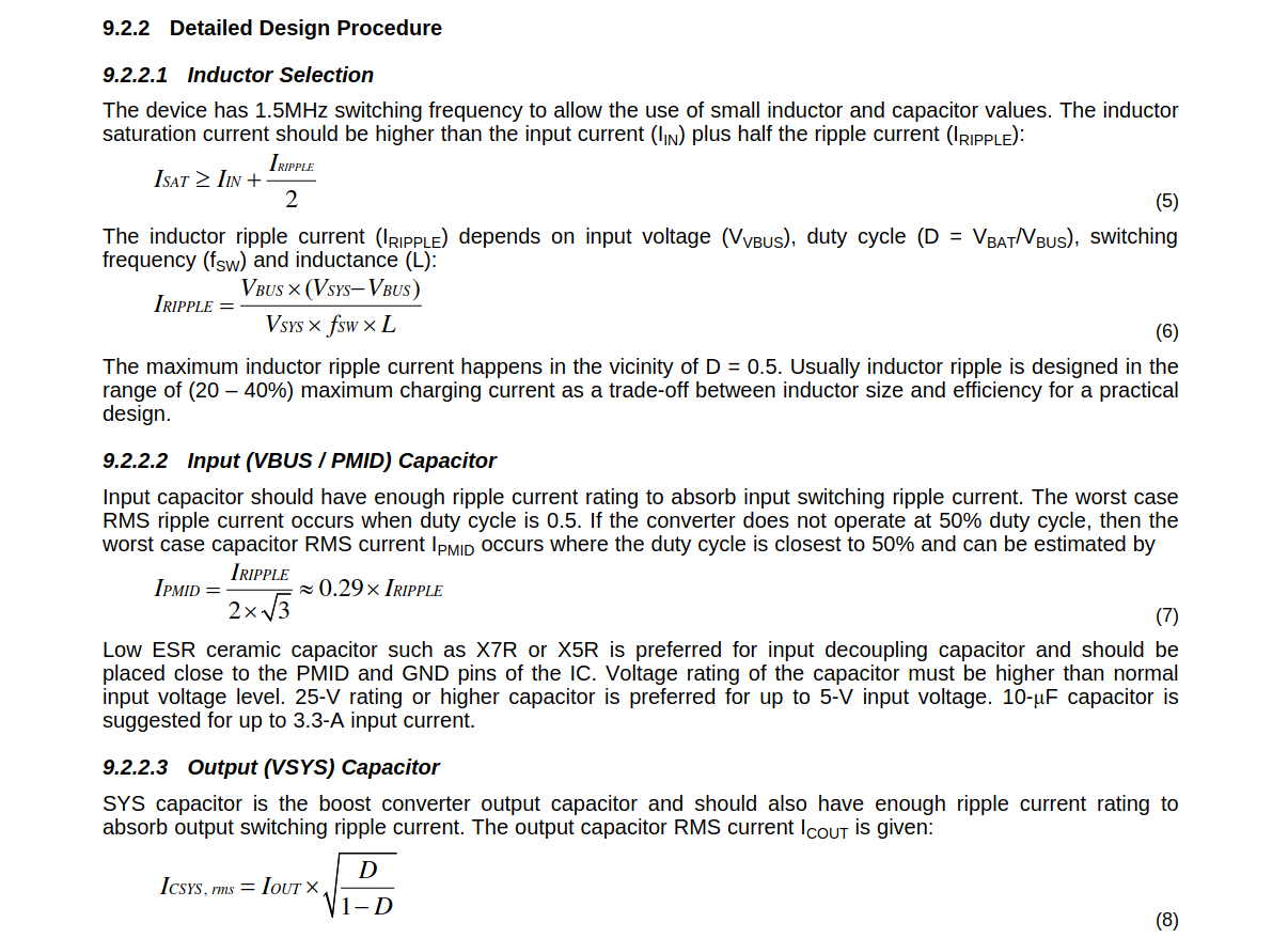
If you need a chip that has a reference schematic that doesn't fit your needs, then you need to do some calculations in order to get the right component values. However, usually you don't have to do that.
#Extra info
If you haven't noticed already, the chip can be connected to a host
through some pins called SDA, SCL, INT, CE, and PG. If you don't know
what they do or want to know what they mean, there's a section in the
datasheet called Pin Configuration and Functions that goes into detail
about what each pin does.
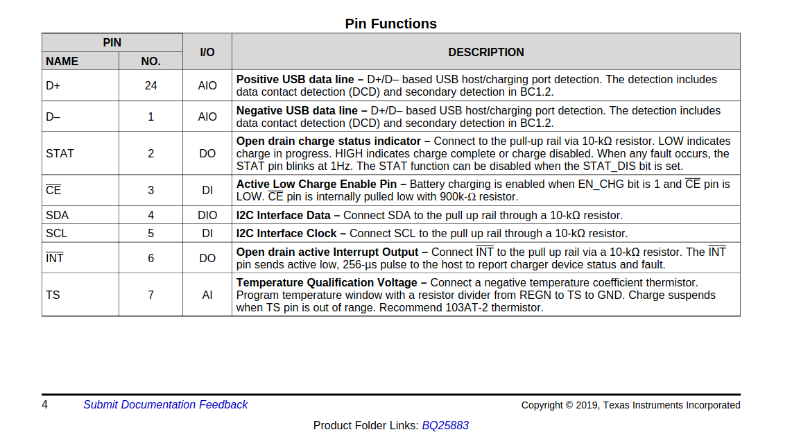
Here we can see that for those pins there are descriptions like
active low, open drain, and I2C. Let's break down what these terms
mean:
Active low
Active low means the pin is "active" (doing its job) when the voltage is LOW (0V or close to ground), not when it's HIGH (3.3V or 5V). Think of it like a backwards switch—when you pull the pin to ground, that's when it triggers the function. Many reset pins work this way: pull the reset pin low to reset the chip, and let it go high to run normally.
Open drain
Open drain is a type of output that can only pull a pin down to 0V (LOW), but cannot push it up to 3.3V (HIGH). Think of it like a one-way switch—it can only connect the wire to ground, not to power. When the switch is "off", the wire is left floating with no connection. This is why open drain pins need a "pull-up resistor"—a resistor that connects the wire to 3.3V and keeps it HIGH when nothing is pulling it down. Multiple chips can share the same wire this way without interfering with each other. See Pull-up Resistors for the full story.
#Communication protocols
Now let's talk about the different ways chips can talk to each other. There are several common protocols you'll encounter:
#I2C/I3C (Inter-Integrated Circuit)
I2C uses only 2 wires: SDA (data) and SCL (clock). Multiple devices can share the same two wires, and each device has a unique address. Think of it like a conference call where everyone shares the same phone line, but each person has a unique ID. Both wires need one pull-up resistor each (in total) in order to function correctly.
Pros:
- Only needs 2 wires regardless of how many devices you connect.
- Built-in addressing system allows multiple devices on same bus.
- Relatively simple to implement.
- Good for sensors and simple peripherals.
Cons:
- Slower than SPI (typically 100 kHz to 3.4 MHz).
- Limited distance—long wires can cause signal problems.
- Can get complex with timing issues and error handling.
- Address conflicts if two devices have the same address.
#SPI (Serial Peripheral Interface)
SPI uses at least 3 wires plus one additional wire for each device: MISO (Master In, Slave Out), MOSI (Master Out, Slave In), SCK (clock), and CS (Chip Select) for each device. It's like having separate phone lines for each conversation.
Pros:
- Much faster than I2C (can go 10 MHz+ easily).
- Full duplex (can send and receive simultaneously).
- Simpler protocol.
- More reliable over longer distances.
Cons:
- Needs more wires (especially with multiple devices).
- No built-in error checking.
- Only one master device allowed.
- Can use up many pins quickly with multiple devices.
#UART (Universal Asynchronous Receiver-Transmitter)
UART uses 2 wires: TX (transmit) and RX (receive). It's a point-to-point connection between two devices, like a private phone call.
Pros:
- Very simple—just 2 wires.
- No clock signal needed (asynchronous).
- Long distance capable with proper drivers.
- Universal—almost every microcontroller has it.
- Good for debugging and console output.
Cons:
- Only connects two devices directly.
- Both devices must agree on baud rate (how fast the data goes) beforehand.
- No built-in error correction.
- Can lose sync if timing is off.
#USB (Universal Serial Bus)
USB uses 2 data wires (D+ and D-) plus power and ground. It's like a smart postal system that can handle packages of different sizes and priorities.
Pros:
- Standardized connector and protocol.
- Provides power to devices.
- Hot-pluggable (can connect/disconnect while powered).
- High speed (up to 10 Gbps on USB 3.1).
- Built-in error correction and flow control.
- Can connect many devices through hubs.
Cons:
- Complex protocol requiring dedicated hardware/software.
- More expensive to implement.
- Requires specific connectors and cables.
- Power management can be tricky.
- Not suitable for real-time applications due to variable latency.
We will not be connecting the USB to the battery charging chip as we need
to connect the STM32 to USB-C to be able to program it. Looking through
the datasheet, it says that those pins are used to determine how much
current can be used. However, they can also be set through the I2C
interface that the IC has, so we can change that later with the STM32.
#Copying the reference schematic
#Wire the charger with net labels
-
Now that we know that the schematic suits our needs, we can start copying it in KiCad. When copying a schematic from a datasheet, any pins that can be connected externally should use
Net Labelslike so (obviously with the pull-up resistors added later):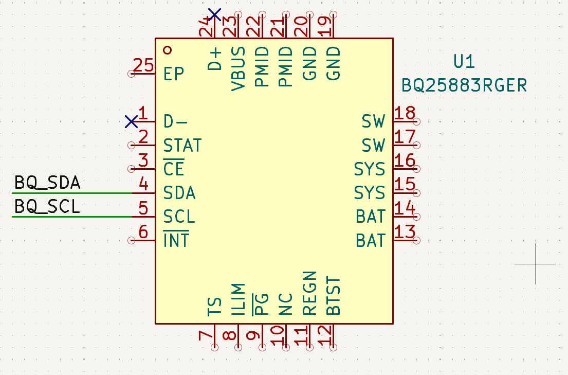
#Separate grounds
Also, because we are dealing with power, we have to use separate grounds
such as power ground and digital ground. Usually, for most chips, we
will use the digital ground. However, sometimes we have to work with
power components and need to have a cleaner ground reference. In the
datasheet, you can see that there are different symbols for ground.
Digital ground is used for all the digital components like microcontrollers, sensors, and logic chips. Digital circuits switch on and off rapidly, creating noise on the ground plane. This is fine for digital circuits since they only care about HIGH (1) or LOW (0), not the exact voltage.
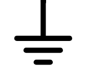
Power ground is used for high-current circuits like motor drivers, charging circuits, and voltage regulators. These circuits can draw lots of current, creating voltage drops and noise in the ground connections. Keeping them separate prevents this noise from affecting sensitive circuits.

#Why separate them?
The noise from digital switching or high-current power circuits can interfere with sensitive analog measurements from the sensors.
The trick is to keep these grounds separate on the PCB traces but connect
them together at a single point. The datasheet says to connect them below
the thermal pad (a conductive area under ICs to dissipate heat/reduce
noise) of the chip. This gives each type of circuit its own clean ground
reference while still maintaining a common ground for the entire board.