
Before we start routing, let's configure the Design Rules. These are
rules that KiCad has to impose certain restrictions like spacing between
components and track width and via size, among other things. It is also
where we can add default sizes for vias (holes that connect tracks
between layers) and tracks (copper lines that connect components).
#Add pre-defined sizes
-
Go to the
Pre-defined Sizessection: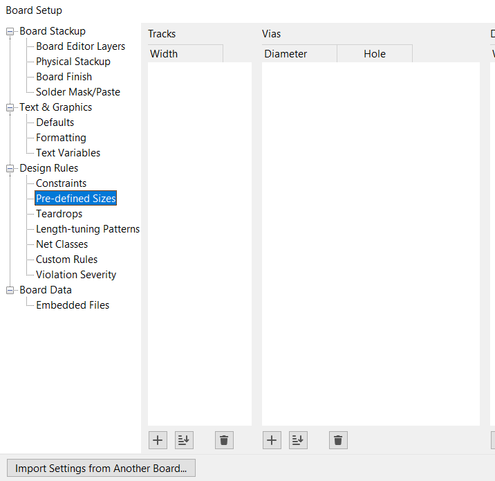
-
I am going to add
0.6mm,0.4mmand0.2mmtrack widths. For vias, I usually go with vias that have0.6mm Diameter / 0.3mm Holeand0.4 Diameter / 0.2mm Hole.
#Loosen constraints for smaller vias
-
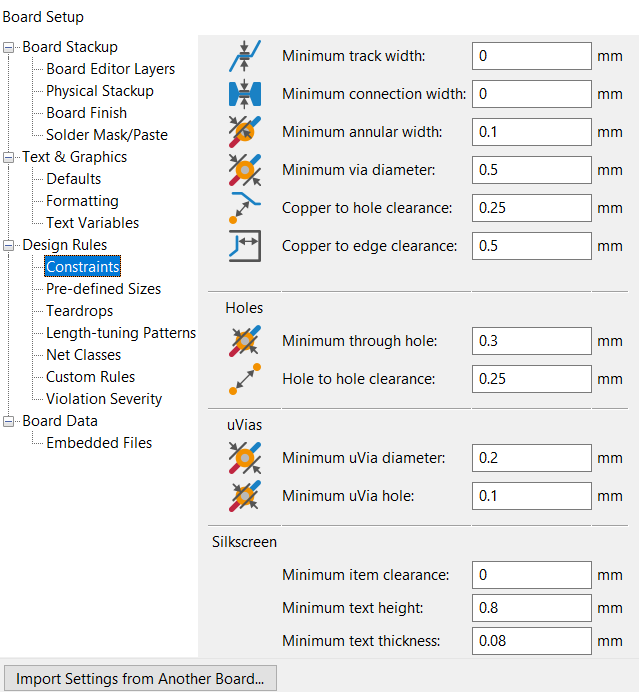
Now after that we have to edit the
constraintsof the board so that KiCad doesn't throw an error when we try to place them. Go to theBoard Setupand thenConstraints.
-
Here we are going to change a couple of settings due to the size of our board. We need to be able to place smaller vias and traces, so change the
Minimum via diameterto0.4mmand theMinimum through holeto0.2mm. After that's done, click OK and you can start routing!
#How to route
Basically connect each of the pads to their connections and try to use as few vias as possible. I usually try to route the signal stuff (USB, sensors, microSD, crystals, etc.) first and then the power.
(Press x to start routing or use the buttons on the side).
#Route the USB-C differential pair
-
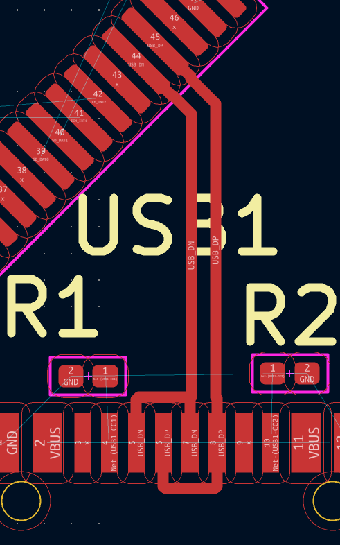
Starting with the USB-C data lines, these are what's known as a
differential pair, so they have to be the same length as they carry a signal that needs to be in sync with the other and the only way for that to happen is if they're the same length. Start connecting them like so: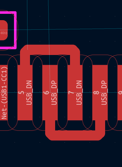
-
Then go to
Route > Route Differential Pair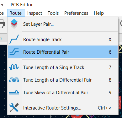
-
and then click on the USB_DP to the far right:
-
Then route it to the STM32. That's basically the only component that needs differential routing.
Moving on, just some general tips. I personally like to use 0.6mm or
0.4mm width for power stuff, mainly anything that runs either
5V (0.6mm) or 3.3V (0.4mm), and
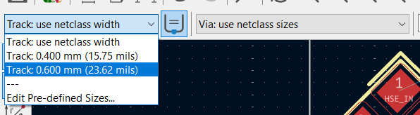
you can change the track width or via size from these drop downs at the
top.
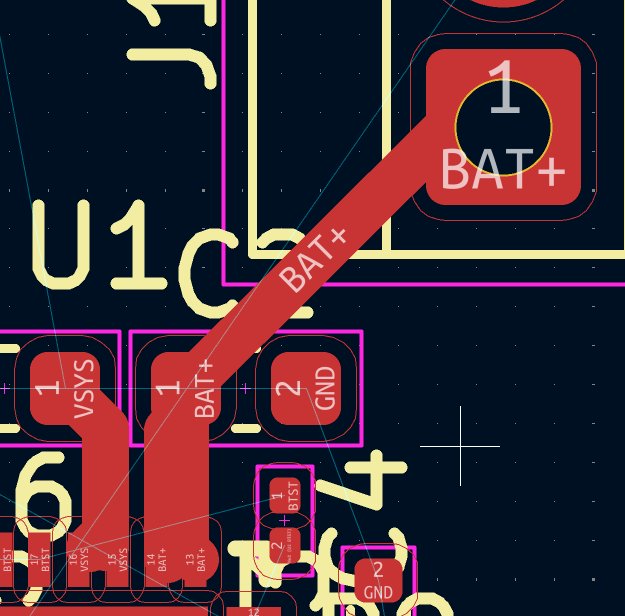
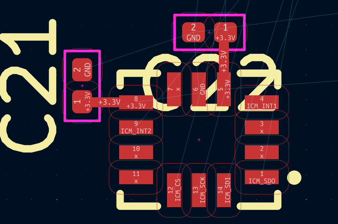
I also like to do the same as in the layout where I route all of the passive components to their respective ICs before then routing those groups together. For example, routing the decoupling capacitors to the IMU before connecting it to the STM32:
You might have to rotate components as well to get a good placement. For vias, I aim to use a maximum of 2 per line like so:
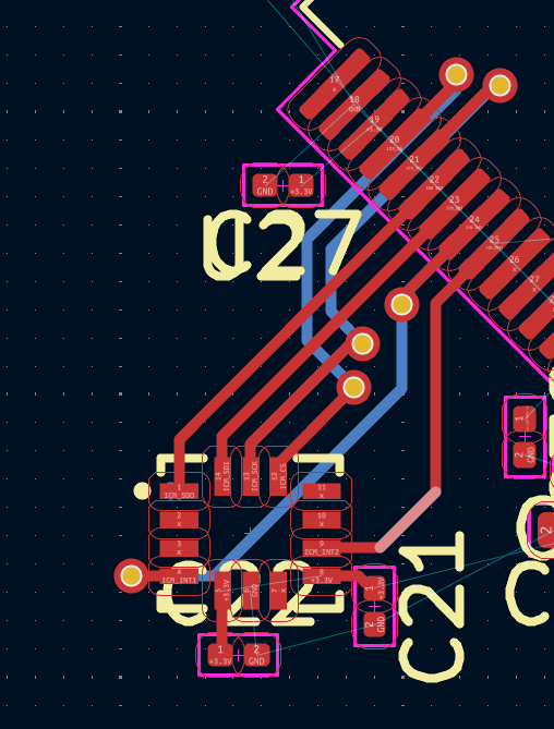
Don't worry about connecting the GNDs for now, as we are going to use
what's called a ground plane (a copper area of GND that can connect to
pins/pads).
#Handle tight-clearance vias
-
Sometimes for VBUS on USB-C or any other component, you might have vias that can't pass through, so I added a
0.3mmtrack width in the board settings and it works: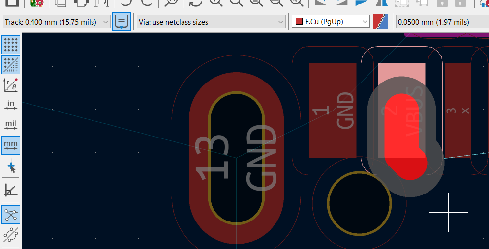
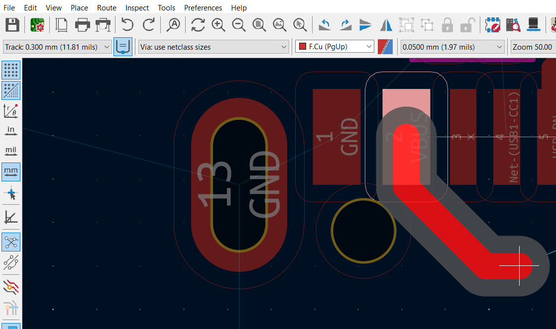
-
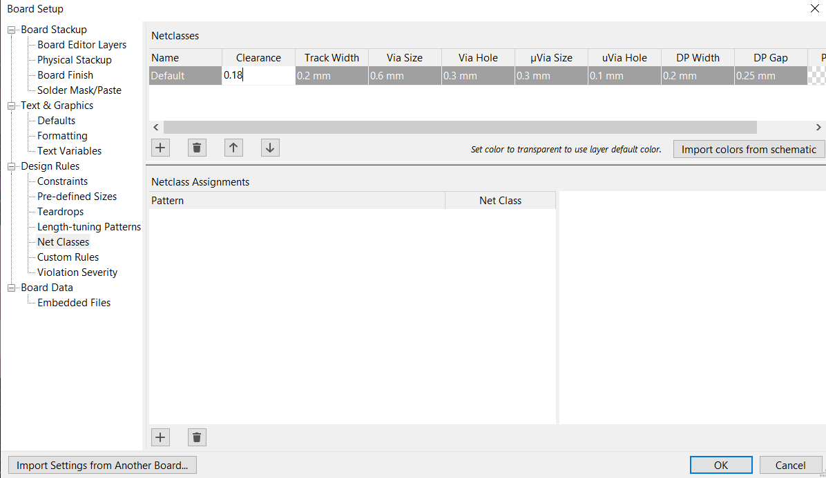
If KiCad doesn't let you place a via on a pad for whatever reason, you can edit the clearance in
Board Setup > Net Classes. I set it to 0.15, but try not to set it any lower as the minimum for JLCPCB is0.1mm: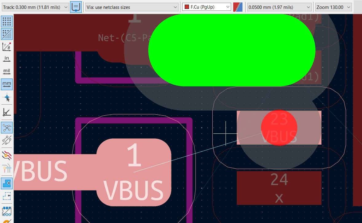
#Route the charger, sensors, and microSD
-
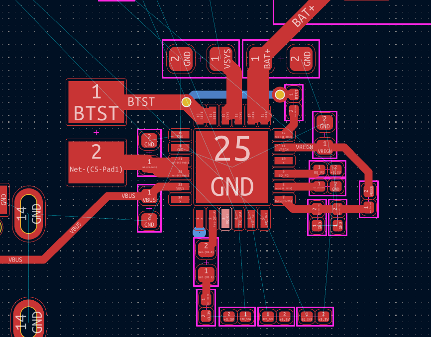
This is how I routed the Battery charger:
-
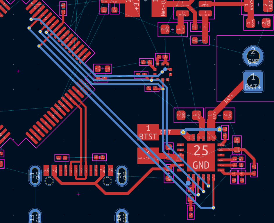
See how I used wider traces for power lines and thinner traces for the other pins. I plan on wiring the I2C lines and INT pins connecting to the BMP580 like so:
-
I connected them to the STM32 through the underside to save space (very useful sometimes). Also, I hid the silkscreen layer so that I can route easier.
-
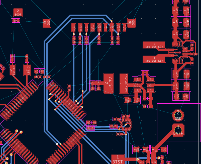
Then routed the microSD card:
#Route the 3.3V rail
- Then finally I routed the 3.3V line, using 0.6mm tracks and then branching off into smaller 0.3mm tracks to connect to the different ICs.
After routing your board should look something like this:
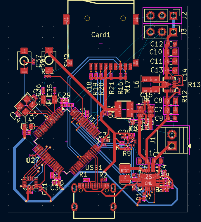
#Ground pours
Now we are going to add the ground pours. This is so that we don't have to manually connect all of the ground pads and it also helps with interference and noise across the board.
#Draw the filled zone
-
Go to the right and click on
Draw filled zonesand click on one corner and a window should pop up: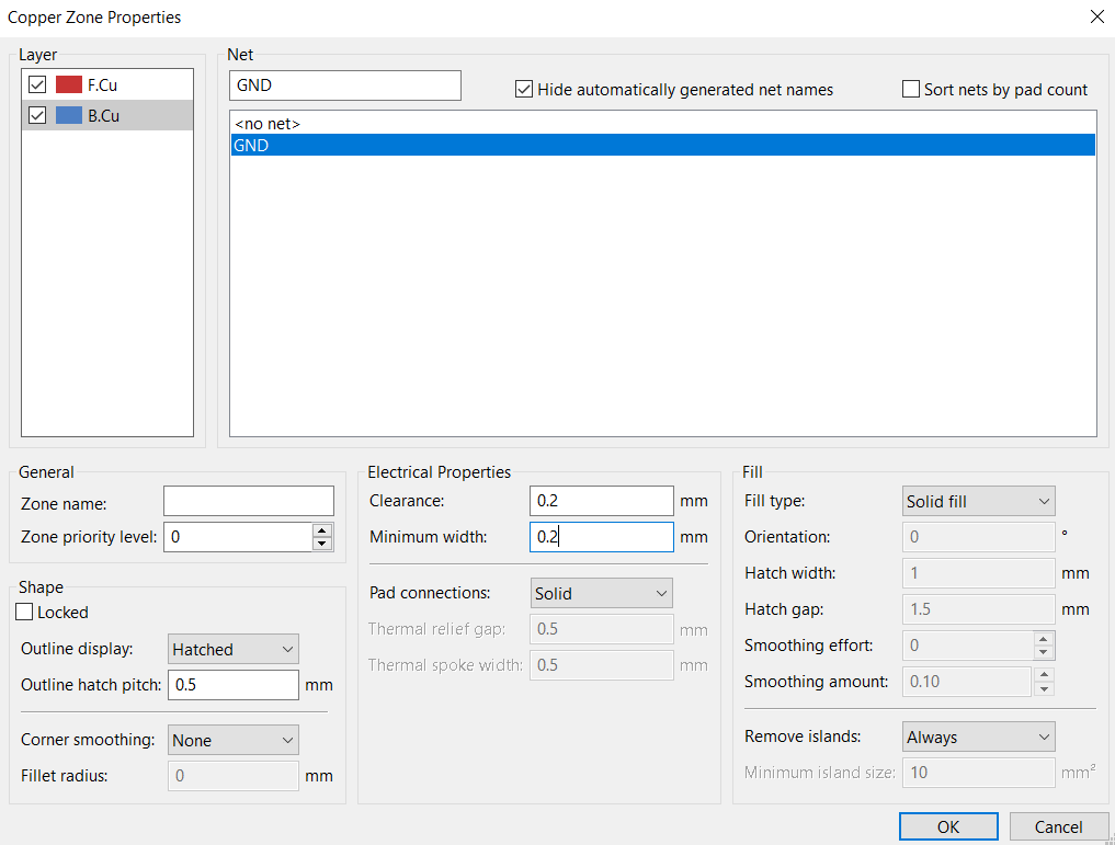
-
Here you need to select both layers of copper and select the GND net. Then you need to change the clearance and minimum width to both 0.2mm and also change the
Pad connectiontoSolidorThermal reliefs. Solid allows the ground plane to connect to the pads better but Thermal reliefs is good if you need to solder/fix the board as the solid ground plane makes it difficult to heat up specific components. For this tutorial I am going to useSolidbut feel free to useThermal reliefsif you want to be able to solder it later. Press OK and start creating the zone like so: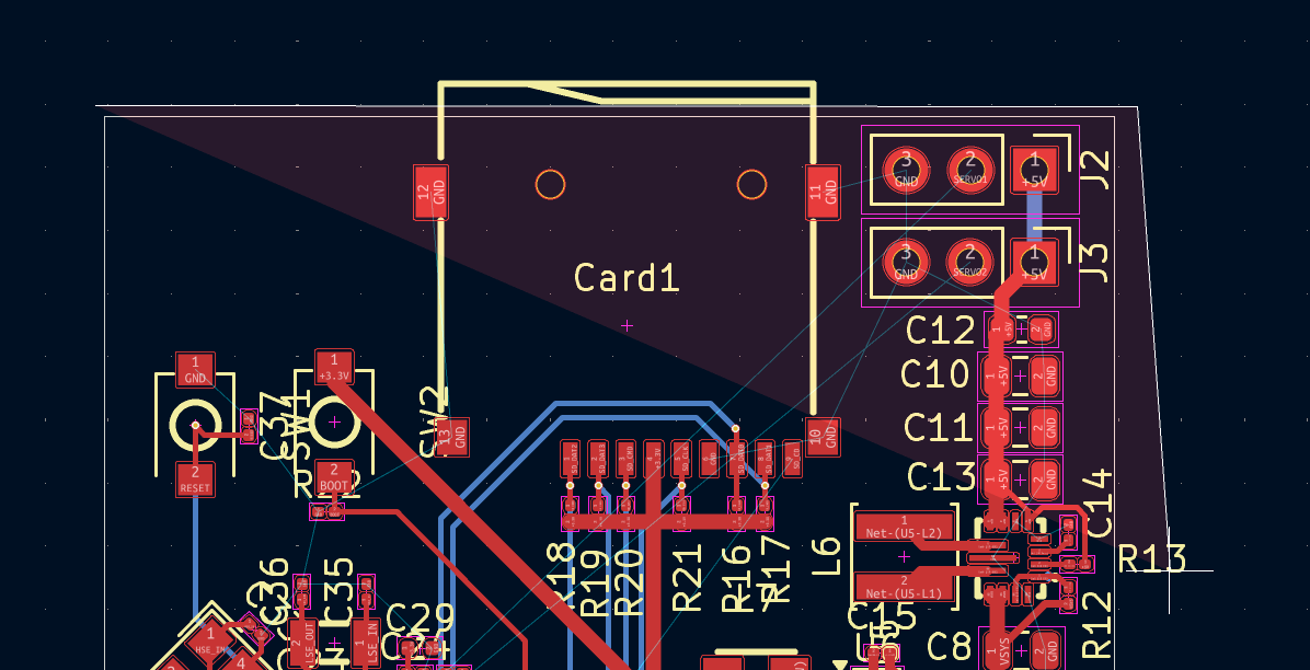
-
You want it to look something like this:
-
Then press
bon your keyboard and it should fill the zone automatically (Ctrl-bto clear them).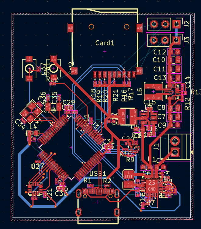
Now you should check if you have any ratlines (blue lines that signal
unconnected pins) and fix them. In my case, I forgot to connect the
servos so I will do that now.
#Add stitching vias
-
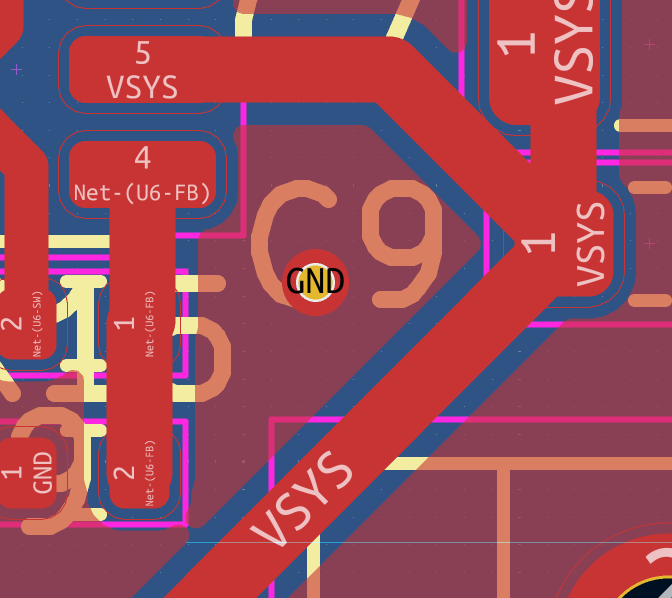
Now you need to check if there are any holes that don't have any ground plane and add a
stitching via(via that connects ground/power planes to cover everything) like so: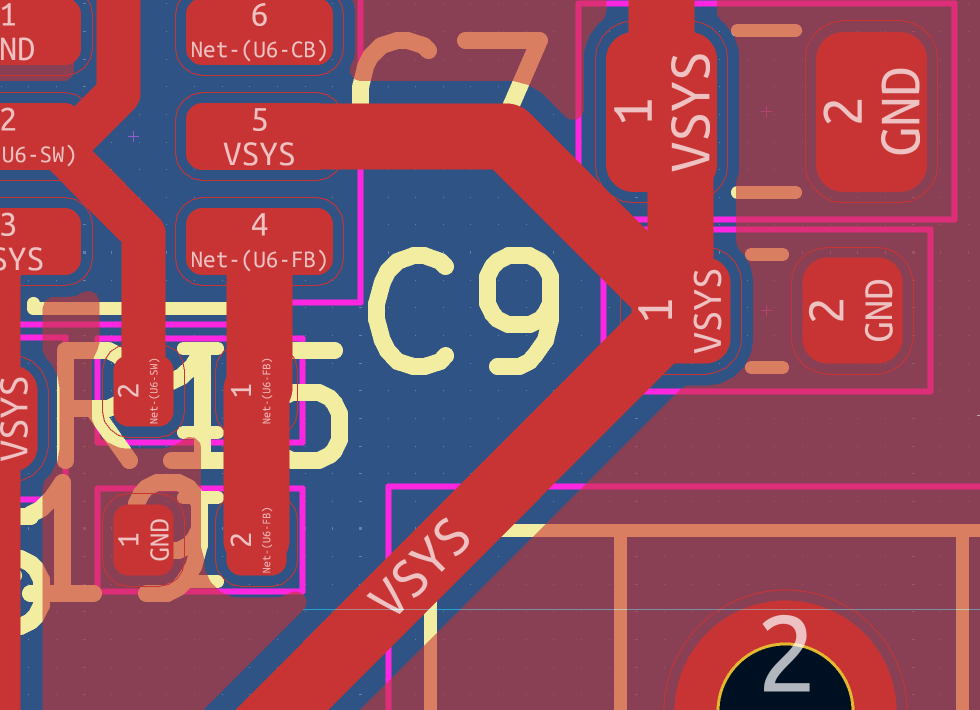
-
You also might see a ratline connecting a piece of the ground plane. This usually means that you need a stitching via in that area.
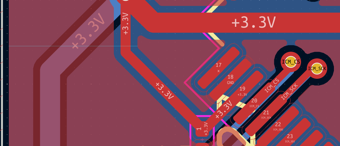
-
As you can see, the ground plane connecting to Pin 18 isn't connected to the rest of the ground plane, so we need to add a stitching via there like so:
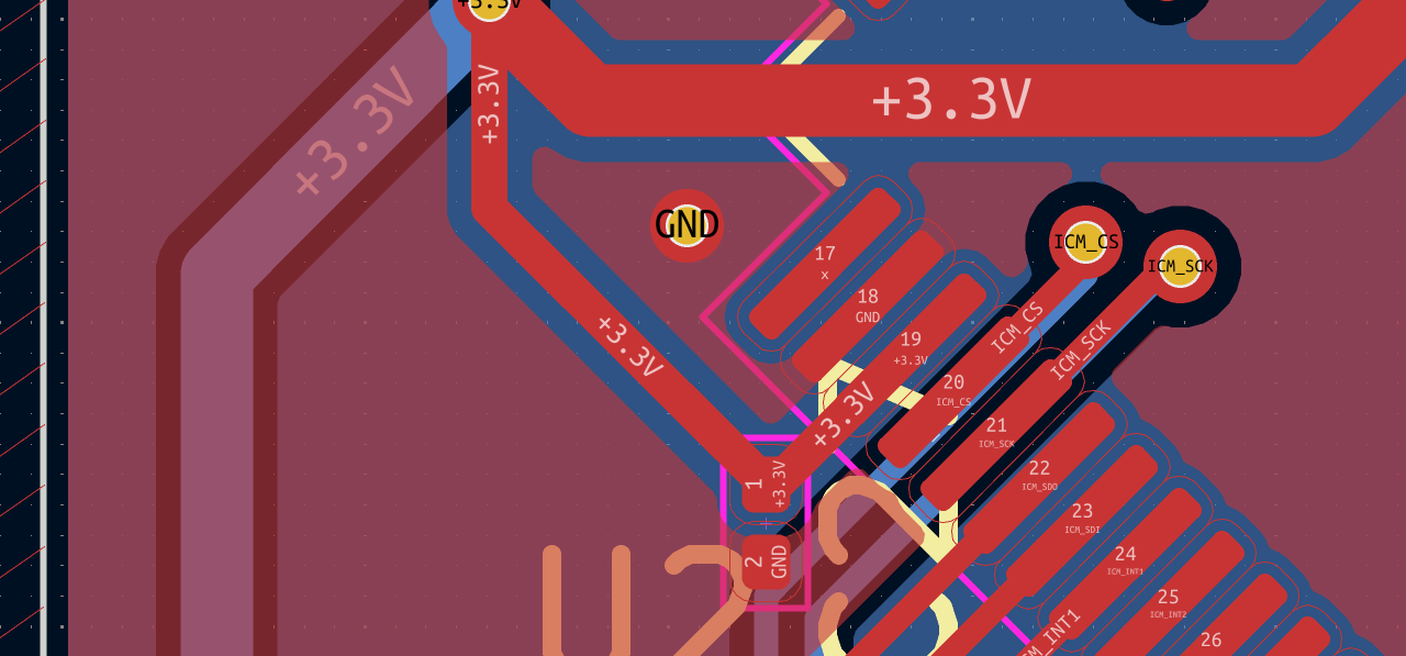
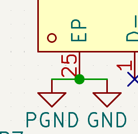
Also Notice how I didn't connect the grounds together and connected both PGND and GND, that was made automatically by KiCad when I connected the EP Pin of the battery charger:
#DRC
#Run design rule check
-
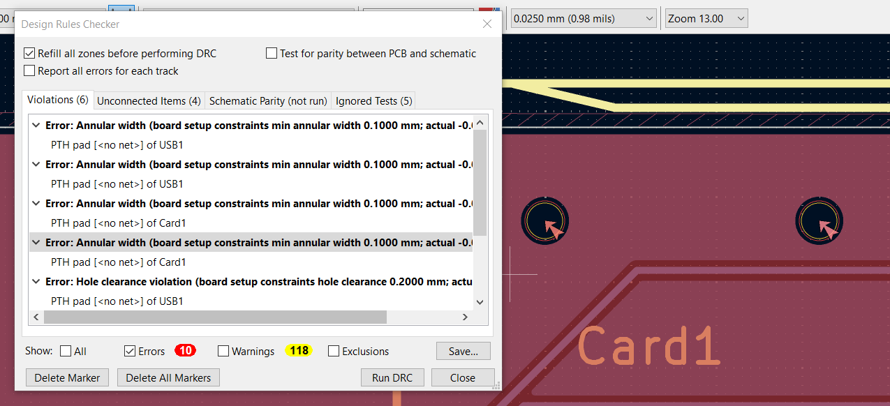
After connecting everything we are going to run
Check DRCwhich basically checks the design rules and makes sure our board is ready for production.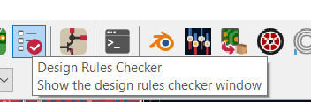
-
Then click on
Run DRC: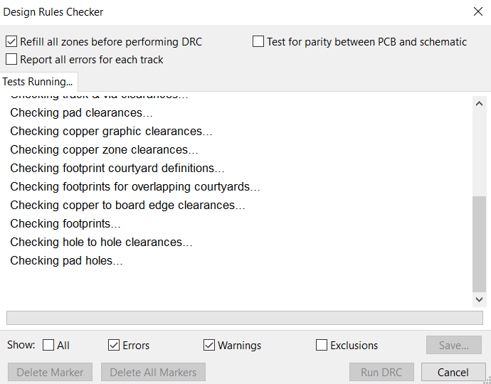
-
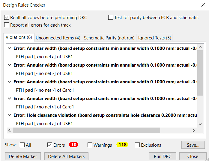
Unselect the warnings and look at the errors. If there are any errors about unconnected pads then you should probably go back and make sure that everything is connected. There are some errors but those are from the parts that we imported like the USB-C and microSD card that KiCad is complaining about the holes:
-
Those errors are safe to ignore but any others you should probably fix.